When a transistor is operated with no emitter degeneration resistor, its transconductance is the following,
\begin{align*}
g_m &= \dfrac{ \partial I_C }{ \partial V_{BE} } \\
&= \dfrac{\partial}{\partial V_{BE}} I_s exp( \frac{V_{BE}}{V_T} ) \\
&= I_s exp( \frac{V_{BE}}{V_T} ) \cdot \dfrac{\partial}{\partial V_{BE}} \frac{V_{BE}}{V_T} \\
&= I_s exp( \frac{V_{BE}}{V_T} ) \cdot \frac{1}{V_T} \\
g_m &= \dfrac{I_C}{V_T} \\
\end{align*}
%\[ \color{red}{ \fbox{ $ g_m = \dfrac{I_C}{V_T}$ } }\]
Emitter Degeneration
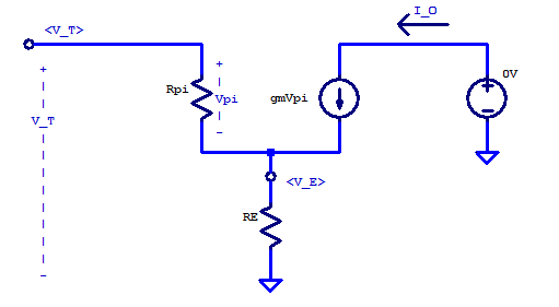
The addition of a series resistor from the emitter terminal to ground, is often refereed to as emitter degeneration. When \( R_E\) is included the net effect is to degenerate the forward transconductance \( (g_m)\) of the transistor. A small-signal model of a transistor with emitter degeneration is shown in the figure below.
 To solve the degenerated transconductance of the transistor the output current \(I_O\) must be determined as a function of input voltage \(V_T\). Beginning with KCL at the \( V_E\) node,
\[ \frac{V_E}{R_E} + \frac{V_E}{r_o} + \frac{V_E – V_T}{r_\pi} +1 – 1 + g_m( V_T – V_E) = 0 \]
\[ V_E \left( \frac{1}{R_E} + \frac{1}{r_o} + \frac{1}{r_\pi} + g_m \right) = V_T \left( \frac{1}{r_\pi} + g_m \right) \]
\[ V_E = \dfrac{1/r_\pi + g_m}{1/R_E + 1/r_o + 1/r_\pi + g_m} V_T \]
\begin{align*}
I_O &= g_m V_\pi – \frac{V_E}{r_o} \\
&= g_m ( V_T – V_E ) – \frac{V_E}{r_o} \\
&= g_m \left( V_T – \dfrac{1/r_\pi + g_m}{1/R_E + 1/r_o + 1/r_\pi + g_m} V_T \right) – \dfrac{1/r_\pi + g_m}{\left(1/R_E + 1/r_o + 1/r_\pi + g_m\right) r_o } V_T \\
&= g_m \left( \dfrac{1/R_E + 1/r_o + 1/r_\pi + g_m – 1/r_\pi – g_m}{1/R_E + 1/r_o + 1/r_\pi + g_m} V_T \right) – \dfrac{1/r_\pi + g_m}{\left(1/R_E + 1/r_o + 1/r_\pi + g_m\right) r_o } V_T \\
&= g_m \left( \dfrac{1/R_E + 1/r_o }{1/R_E + 1/r_o + 1/r_\pi + g_m} V_T \right) – \dfrac{1/r_\pi + g_m}{\left(1/R_E + 1/r_o + 1/r_\pi + g_m\right) r_o } V_T \\
&\simeq g_m \left( \dfrac{1/R_E + 1/r_o }{1/R_E + 1/r_o + 1/r_\pi + g_m} V_T \right)\\
&\simeq g_m \left( \dfrac{1 }{1+ g_m R_E} \right) V_T \\
\end{align*}
\begin{align*}
g_{m,degen} &= \frac{\partial I_O}{ \partial V_T } \\
&= \frac{\partial}{ \partial V_T } \left( \dfrac{g_m }{1+ g_m R_E} \right) V_T \\
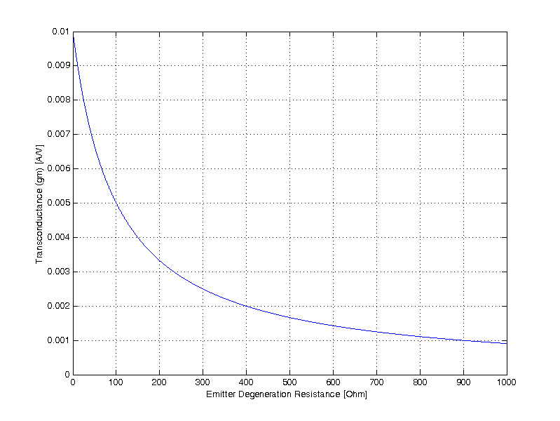
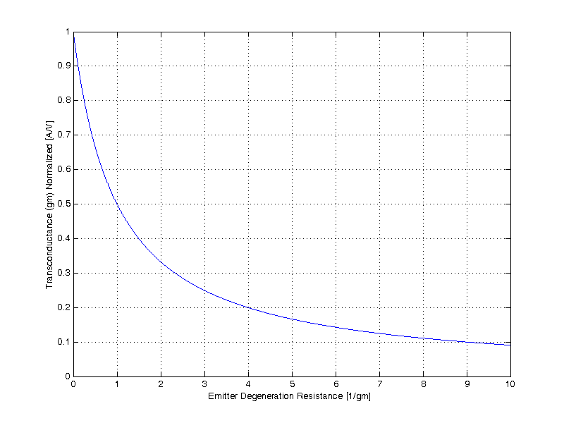
g_{m,degen} &= \dfrac{g_m}{1 + g_m R_E}
\end{align*}
When the degenerated transconductance approaches 1/Re, a low gain CE voltage amplifier can be easily constructed as
\begin{align*}
A_V &= – g_{m,degen} R_L \\
&= \dfrac{g_m}{1 + g_m R_E} R_L \\
A_V &\simeq – \dfrac{R_L}{R_E}\;,\;\;\; \textrm{For \(R_E\) >> \(1/g_m\) }
\end{align*}
Some common examples where emitter degeneration may be applied:
- Increasing the output impedance of an amplifier
- Increasing the input impedance of an amplifier
- Improving the stability of a DC operating point
- Lowering the DC gain
- With a bypass capacitor in parallel to \(R_E\), the HF \(g_m\) can be maintained
- Low gain amplifier as \( |A_v| = R_L / R_E \)