DAC Specifications – Ideal Case

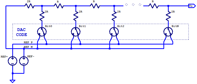
A Digital to Analog Converter (DAC) in the ideal case, provides a unique transform from a digital code to an analog voltage ratiometric to a supplied voltage reference. Several codings of the digital value are available. Two of the simplest codings are unsigned binary and unsigned fractional binary. Other possible codings include: two’s complement, sign-magnitude, one’s complement, and gray code. In practice, only unsigned binary and two’s complement (signed binary) are commonly employed in a DAC. For both the signed and unsigned cases, the integer and fractional codings share the same binary representation. For example, a 3-bit DAC has the response shown in the table below.

DAC Response to Integer and Fractional Codes
Decimal Fractional Unsigned Binary Fractional Binary DAC Output
0 0/8 000 0.000 \( 0/8 \; V_{REF} \)
1 1/8 001 0.001 \( 1/8 \; V_{REF} \)
2 2/8 010 0.010 \( 2/8 \; V_{REF} \)
3 3/8 011 0.011 \( 3/8 \; V_{REF} \)
4 4/8 100 0.100 \( 4/8 \; V_{REF} \)
5 5/8 101 0.101 \( 5/8 \; V_{REF} \)
6 6/8 110 0.110 \( 6/8 \; V_{REF} \)
7 7/8 111 0.111 \( 7/8 \; V_{REF} \)

Continue reading “DAC Specifications – Ideal Case”

R2R DAC

A Digital to Analog Converter (DAC) is a critical building block in almost every modern electronic system today. A DAC translates a digital code to an analog output voltage. For a typical uni-polar DAC, the DAC code maps to an output voltage spanning 0 V to the DAC’s associated voltage reference’s potential \(V_{REF}\). When a resistor ladder of two unique resistance quantities, namely R and 2R are chosen, some admirable attributes are obtained which are well suited to the design of a DAC. The schematic below is a simplified schematic of an R2R DAC; the DAC switches and voltage reference are idealized.

An N-bit R2R DAC, with single-ended unipolar output.

Continue reading “R2R DAC”

GPIO Output Resistance

In this blog post, we will take a look at the output resistance of General Purpose Input Output (GPIO) pins. For the purposes of discussion, the Microchip PIC24FJ32GA002; a 16-bit micro-controller available in a 28-pin DIP package, will be analyzed in detail related to its GPIO structure. In general for digital logical, three output states are available: output low, output high, and high-impedance. A simplified circuit for the output portion of a GPIO pin is shown below.Simplified schematic model of a GPIO pin.

Continue reading “GPIO Output Resistance”

LC Butterworth – Component Sensitivity

Monte-Carlo Simulation

Each of the discrete filter components is assumed to be normally distributed with \(\sigma = 0.02 \mu \).

\begin{align*}
R_S &\sim \mathcal{N}\left( 1, (0.02)^2 \right) \\
R_L &\sim \mathcal{N}\left( 1, (0.02)^2 \right) \\
L_1 &\sim \mathcal{N}\left( 1.6180, (1.6180 \cdot 0.02)^2 \right) \\
L_2 &\sim \mathcal{N}\left( 1.6180, (1.6180 \cdot 0.02)^2 \right) \\
C_1 &\sim \mathcal{N}\left( 0.6180, (0.6180 \cdot 0.02)^2 \right) \\
C_2 &\sim \mathcal{N}\left( 2, (2 \cdot 0.02)^2 \right) \\
C_3 &\sim \mathcal{N}\left( 0.6180, (0.6180 \cdot 0.02)^2 \right) \\
\end{align*}

Continue reading “LC Butterworth – Component Sensitivity”

LC Butterworth Filter

Physical synthesis of a Butterworth filter requires components which can be interconnected to form complex poles (dampened harmonic oscillators). A passive arrangement of resistors and capacitors can form arbitrary real valued poles and zeros; however a passive RC network cannot synthesize complex poles. The natural choice for passive components which can synthesize oscillators, are inductors and capacitors. An immediate benefit of choosing an LC network for synthesis, is that the network in the ideal case is lossless. Allowing for low insertion-loss in the pass-band, and maximizing power transfer from source to load.

The most common network structure for synthesis is a series inductor and shunt capacitor ladder. A LC ladder of arbitrary order \(n\), is shown in the figure below.

Schematic of an LC butterworth filter.

Continue reading “LC Butterworth Filter”

RC Second Order Low-pass Filter

One of the simplest designs for a second order low-pass filter, is a RC ladder with 2 resistors and 2 capacitors. A drawback to this filters simplicity is that it requires a near ideal voltage source and a load with extremely high input impedance (ex. a buffer amplifier). A schematic of a second order RC low-pass filter is shown in the schematic below.  Continue reading “RC Second Order Low-pass Filter”

RC First Order Low-pass Filter

General Case

For the general case of applying a filter between some signal source and load point, the solution space is constrained when the design is limited to only resistors and capacitors. For the sake of discussion, consider the schematic below. Here the signal source \(V_S\) has an output resistance of \(R_S\) and the filter is loaded by the input input resistance of the proceeding signal stage.

An RC low-pass filter must operate when presented with finite source and load resistances.

In some cases, the load resistance is negligible. For example the non-inverting input of an op-amp, when configured as a unity gain buffer has very high input resistance and only a small shunt capacitance. The output resistance of an 0p-amp, when operating closed-loop with negative feedback, is also a relatively low output resistance signal source. Other cases which have significant source resistance include a plethora of transducers, such as the electret condenser in a microphone. A load with significant input resistance is a loudspeaker, which provides a load resistance ranging from 4 ohms to 32 ohms.

In the general case, additional resistance in the signal path is often undesirable, as it limits the power transfer capability from source to load. Additional resistance whether it be in series or parallel to the load, yeilds additional signal attenuation from source to load, there by lowering the filtered signal level, which in turns degrades the Signal to Noise Ratio (SNR).

When the source resistance is significant, only an additional capacitor is required.

Continue reading “RC First Order Low-pass Filter”

Butterworth Filter

The Butterworth filter is an interesting filter in that its origin is based on the desire of a particular magnitude function. Butterworth (S. Butterworth, the Engineer in the 1930’s) demonstrated that the magnitude-squared function of

\[ \left| H\left( j \omega \right)\right|^2 = \dfrac{A^2}{1+\omega^{2n}} \]

has many admirable properties for use as a low-pass filter. To maintain consistency with Butterworth’s original paper and most academic treatments of the Butterworth filter, the filter is described as a prototype filter with unity gain and a cutoff frequency of \( \omega_c = 1 \) rad/s.

-The passband is the frequency spectrum of \( 0 \leq \omega \leq 1 \) rad/s

-The stopband is the frequency spectrum of \( \omega > 1 \)

-At the corner frequency \( \omega_c = 1\) rad/s, the magnitude response is always

\[|H(j\omega_c)| = \frac{1}{\sqrt{2}}=\;\; – 3 \text{ dB,  for any filter order n.}\]

-Past the corner frequency \(\omega_c\) the magnitude response declines at a rate of \(-20 n \) dB/decade

-The magnitude response over frequency is monotonic (i.e. flat or decreasing) , thus no ripple.

Continue reading “Butterworth Filter”

Cascading Single Pole Filters

One approach to improving stopband rejection is to cascade several first-order filters, there by achieving the combined rejection of n filters for better stopband rejection. While the implantation of such an arrangement is straight forward, there are some consequences to this approach which will be discussed below.

For a low-pass filter of the form

\[ H(s) = \dfrac{1}{1 + s/p} \]

From control theory the cascaded transfer function is just the multiplication of each filter transform. When each filter has an identical transfer function the overall transfer function is the following

\[ C(s) =  \dfrac{1}{(1 + s/p)^n} \]

Continue reading “Cascading Single Pole Filters”