In this blog post, we will take a look at the output resistance of General Purpose Input Output (GPIO) pins. For the purposes of discussion, the Microchip PIC24FJ32GA002; a 16-bit micro-controller available in a 28-pin DIP package, will be analyzed in detail related to its GPIO structure. In general for digital logical, three output states are available: output low, output high, and high-impedance. A simplified circuit for the output portion of a GPIO pin is shown below.
To be complete, the schematic above would include include additional logic to allow for both the pull-down NMOS and pull-up PMOS to be simultaneously disabled, to achieve a high-impedance state. During normal operation, one can observe that provided the BUFout voltage is between ground and VDD, diodes D1 and D2 are both reverse biased. It is only for invalid logic states, i.e. negative voltages or voltages greater than VDD that diodes D1 and D2 may begin to conduct.
When the GPIO pin is driving an output low, the pull-down NMOS is enabled and the pull-up PMOS is disabled. The output resistance in this case is the \(R_{DSON}\) of the NMOS. A MOSFET has three modes of operation when \( 0 \geq V_{DS} \gt V_{BRKDOWN} \). The three modes of operation, are summarized in the table below
| \(V_{GS}\) | \( V_{DS} \) | Conduction Mode | \(I{ds}\) | Output Resistance |
|---|---|---|---|---|
| \( \lt V_T\) | NA | Cut-off | 0 | Hi-Impedance |
| \( \gt V_T\) | \( \lt (V_{GS}-V_T)\) | Triode/Ohmic | > 0 | Low-Resistance \((R_{DSON})\) |
| \( \gt V_T\) | \( \gt (V_{GS}-V_T)\) | Saturation | > 0 | Hi-Impedance \( (r_o) \) |
For the PIC24, the complete IO module is shown in the figure below.

From the block diagram above, one can see the PIC24 allows for either a direct read of actual IO pin state or of latched output state. When using the IO pin as an output pin, it is advisable to read the latched state versus the actual pin state.
Offset Compensated Ohms
Since a micro-controller is a complete system on chip, it is difficult to isolate the behaviour of the output IO block from the rest of the system. Its not like you can just cut it out and probe it (easily at least). One of the largest non-idealities introduced because of this, is an offset in ground potential. All of the on die processor/system current is sunk through common routing on die and through common ground pins. In order to compensate for this fact, the output resistance must be measured at two bias points. A general test methodolgy for offset compensated ohms is shown in the figure below

Here a programmable bias current is generated with voltage source \(Vs\) and bias resistor \(R_{REF}\). If one has a precision current source, the voltage source, bias resistor, and ammeter may be replaced with a programmable current source. In this proposed implementation only two reasonable accurate measurement instruments (DMMs) are required. The accuracy of the bias resistor and voltage source, are immaterial.
In the figure above, one can see that \(I_{SYS}\) is shunted across \( R_{GROUND}\), which develops an offset potential looking into the IO pin. The total output resistance looking into the IO pin is sum of \(R_{DSON}\) of the NMOS and \( R_{GROUND}\) from die routing, wire bonding, package interconnect, and potentially PCB routing as well. In a typical resistance measurement where a calibrated constant bias current is applied and the resulting voltage is recorded. Resistance is then calculated from Ohms law. For offset compensated ohms, resistance is derived from the I-V slope. A sample dataset taken from a PIC24, applying the offset compensated ohms technique is shown in the figure below.

For this PIC24, we can observe that there is approximately 1.3 mV of offset voltage at IO pin RB15. The output resistance is then the I-V slope from a least-squares fit of the measurement data, which for pin RB15 is 24 Ohms.
Matched Output Resistance
In the ideal case, each of the GPIO cells on die should be completely identical, and consequently each GPIO pin should have the same output resistance. For the PIC24, no specification/guarantee is made to how well each IO pin is matched. The only specification provided is the IO levels for some load current. The table below is taken from the PIC24 datasheet.

Here we can see, that for the case of an Output Low state on an IO pin, the output voltage is < 400 mV while sinking 8.5 mA. While no explicit guaratee that the I-V curve is resistive at \(V_{DS} = 400\) mV. It is an extremely conservative estimate that the threshold voltage \(V_T\) of the output NMOS is not 3.6 – 0.4 = 3.2 V, as the NMOS would be in cut-off for supply voltages less than 3.2 V. Knowing the NMOS must be in triode, we can approximate \( R_{DSON}\) as,
\begin{align*}
R_{DSON} &= \dfrac{V_{OH}}{I_{SINK}} \\
&= \dfrac{400 \text{ mV}}{8.5 \text{ mA}} \\
R_{DSON} &= 47 \text{ }\Omega \\
\end{align*}
We can assert that for \( V_{DD} = 3.6 \) V, the output resistance for an output low logic state is 47 Ohms worst case.
Continuing with using the PIC24 as an example, we will determine how well each GPIO pin is matched in output resistance. An outline schematic of the measurement setup is shown below.
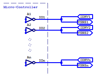
While each IO pin could each be tested simultaneously (provided the total sink/source IO current remains below the PIC24 specification). In this post, each IO pin will be tested consecutively. The pinout of the DUT is shown below

We will focus our analysis on GPIO pins RB6 to RB15 (GPIO pins on the right-hand side of the DIP package).
Following the offset compensated ohms setup above, the I-V curves for IO pins RB6 to RB15 is shown in the figure below. Immediately one can observe two outliers with regards to output resistance. The top black line indicates a higher than average output resistance, and equivalent the lowest blue line demonstrates a lower than average output resistance.
| GPIO Pin | Output Low Res. [Ohms] |
|---|---|
| RB6 | 26.71 |
| RB7 | 26.69 |
| RB8 | 26.73 |
| RB9 | 26.77 |
| RB10 | 26.49 |
| RB11 | 26.46 |
| RB12 | 26.44 |
| RB13 | 26.45 |
| RB14 | 32.84 |
| RB15 | 25.70 |
The mean output resistance of GPIO pins RB6 to RB13 is 26.592 Ohms with a standard deviation of \(\sigma = 0.14 \) Ohms. A plot of each GPIOs output resistance is shown in the figure below.

The results are disheartening in that, pin RB14 has a 24% larger output resistance compared to similar IO pins on PortB. Pin RB15 is approximately 4% lower in output resistance compared to RB6 to RB13.
Does any of this matter? Well, all the IO pins tested certainly meet the specification of having an output resistance less than 47 Ohms. In digital applications pin RB14 will have a 24% slower rise-time, which is more than likely negligible. However in respect to the Homebrew DDS blog series, GPIO pins RB8 to RB15 are one contiguous byte in PORTB which is directly byte addressable. If one were to use pins RB8 to RB15 as switching elements in an R2R DAC, a DAC resistance R, must be chosen to be substantially greater than the 6 Ohm delta between pins.