A Digital to Analog Converter (DAC) is a critical building block in almost every modern electronic system today. A DAC translates a digital code to an analog output voltage. For a typical uni-polar DAC, the DAC code maps to an output voltage spanning 0 V to the DAC’s associated voltage reference’s potential \(V_{REF}\). When a resistor ladder of two unique resistance quantities, namely R and 2R are chosen, some admirable attributes are obtained which are well suited to the design of a DAC. The schematic below is a simplified schematic of an R2R DAC; the DAC switches and voltage reference are idealized.
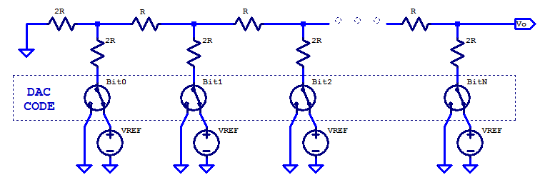
The behavior of such a resistance ladder can be analyzed interactively beginning with the Least Significant Bit (LSB), bit 0. All ladder components proceeding bit 0 are ignored for the time being. The remaining ladder elements for bit 0 are shown in the schematic below.
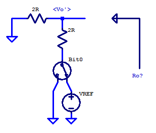
For the purposes of analysis, the output node of bit 0 is labelled as \( V_o’\). It is important to note that \( V_o’\) is the unloaded open circuit voltage when all higher order ladder components are removed. We can first observe that, by inspection the output resistance of bit 0’s ladder elements is
\begin{align*}
R_{out,0} &= ( 2R||2R ) \\
R_{out,0} &= R
\end{align*}
The unloaded output voltage can be solved as simple voltage-divider. Switch bit0 and voltage reference \(V_{REF}\) can be simplified as a voltage source with two voltage states. We introduce a voltage source \(V_{bit,0}\) which has a value of either 0 V or \(V_{REF}\). The unloaded circuit voltage of bit0 is then,
\begin{align*}
V_o’ &= \left(V_{bit,0}\right) \dfrac{2R}{2R+2R} \\
V_o’ &= \dfrac{ V_{bit,0} }{2} \\
\end{align*}
The ladder elements for bit0 and below (nothing) can be modeled as the Thevenin equivalent circuit shown in the figure below.
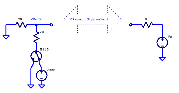
We can see bit 0 has an unloaded voltage of either 0 or \( V_{REF}/2 \), with an output resistance of R.
Continuing our analysis, we include all ladder elements up until bit 1. Our analysis is greatly simplified by including the Thevenin equivalent model for bit 0, as shown in the figure below.
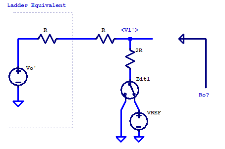
For the 2R2 ladder up until bit1 we can asses by inspection that the output resistance is
\begin{align*}
R_{out,1} &= ( 2R||2R ) \\
R_{out,1} &= R
\end{align*}
The unloaded output voltage can be solved by applying KCL at the \( V_1’\) node as,
\[ \dfrac{V_1′ – V_0′}{2R} + \dfrac{V_1′ – V_{bit,1}}{2R} = 0 \]
\[ V_1′ = \dfrac{V_0′}{2} + \dfrac{V_{bit,1}}{2} \]
Continuing onto bit2, we simplify the lower ladder elements as the unloaded voltage at bit1 with its output resistance \(R\). A simplified schematic for the ladder up to bit2 is shown below
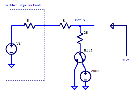
We can see that, once again the output resistance is \(R\). The unloaded circuit voltage \(V_2’\) is by KCL,
\[ \dfrac{V_2′ – V_1′}{2R} + \dfrac{V_2′ – V_{bit,2}}{2R} = 0 \]
\[ V_2′ = \dfrac{V_1′}{2} + \dfrac{V_{bit,2}}{2} \]
This pattern continues for an indefinite number of R-2R elements. The output resistance of any length of R2R ladder is always R. The relation for output voltage can be seen, by expanding the output voltage at bit2 as
\begin{align*}
V_2′ &= \dfrac{V_1′}{2} + \dfrac{V_{bit,2}}{2} \\
V_2′ &= \dfrac{V_0′ + V_{bit,1}/2}{2} + \dfrac{V_{bit,2}}{2} \\
V_2′ &= \dfrac{V_{bit,0}}{8} + \dfrac{V_{bit,1}}{4} + \dfrac{V_{bit,2}}{2} \\
\end{align*}
The output voltage of an R2R ladder is a binary weighted combination of the DAC bits. As an example, a 3-bit R2R DAC would have an output voltage of
\[ V_{out} = \dfrac{ 4V_{bit,2} + 2V_{bit,1} + V_{bit,0} }{8} \]
A full table of all DAC codes and output values for a 3-bit DAC is shown below
| DAC Code | Output Voltage |
|---|---|
| 000 | \( 0/8 \) \( V_{REF} \) |
| 001 | \( 1/8 \) \( V_{REF} \) |
| 010 | \( 2/8 \) \( V_{REF} \) |
| 011 | \( 3/8 \) \( V_{REF} \) |
| 100 | \( 4/8 \) \( V_{REF} \) |
| 101 | \( 5/8 \) \( V_{REF} \) |
| 110 | \( 6/8 \) \( V_{REF} \) |
| 111 | \( 7/8 \) \( V_{REF} \) |
From the analysis in this post we can infer one of the key specifications for a DAC, namely its resolution. For an R2R DAC its resolution is
\[ \Delta \text{LSB} = V_{REF} \dfrac{1}{2^N} \]
Where N is the number of R-2R elements in the DAC’s R2R ladder.
As an example, suppose we wish to have a DAC with an output range of 0 V to 2.5 V and a resolution of 1 mV. Naturally we choose an R2R DAC, and thus require a 2.5 V reference. The number of bits required for the proposed R2R DAC is then,
\begin{align*}
N &= \log_2\left( \dfrac{2.5 \text{ V}}{1 \text{ mV}}\right) \\
N &= 11.3 \text{ bits} \\
\end{align*}
Rounding N up to the next whole integer value, yields a 12 bit DAC. The effective resolution of the proposed DAC is then,
\begin{align*}
\Delta \text{LSB} &= \dfrac{2.5 \text{ V}}{2^{12}} \\
\Delta \text{LSB} &= 610 \text{ uV} \\
\end{align*}
Thevenin
Yes, thank you so much.