Basic Solar Panel Model

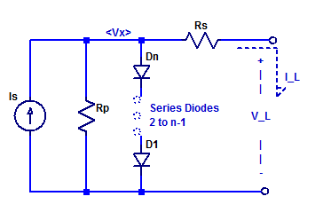
A solar panel is constructed as a series string of discrete solar cells (or potentially parallel array). Each cell of the series string has its own series resistance and shunt resistance in addition to the diode junction. Loosely speaking one can construct a circuit equivalent model of a solar panel as shown in the figure below.
Simplified Schematic of an N Cell Solar Panel.

Here the panel is constructed with N equal diode junctions all sharing one common photo current source \(I_S\). Continue reading “Basic Solar Panel Model”

Maximum Power Point of Diode Shunted Current Source

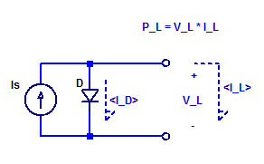
In this post, the maximum power point (MPP) of a diode shunted current source will be assessed and modeled. A solar cell in its simplest description is merely a semiconductor diode. When the cell’s junction is illuminated, a photo current \(Is\) is produced. A basic schematic model of an ideal solar cell is shown in the figure below.

Schematic of Diode Shunted Current Source.

For diode forward voltages \(V_D\) greater than a few \( \eta V_T\), such as 100 mV, the diode equation is approximately equal to,

$$ I_D \simeq I_o exp\left( \dfrac{V_D}{\eta V_T} \right) $$ Continue reading “Maximum Power Point of Diode Shunted Current Source”

Maximum Power Point of a Current Source

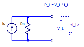
While it is true an ideal current source can deliver an infinite amount of output power (at a constant current), as the output compliance voltage is infinite. A real current source has a finite output resistance which limits the maximum output voltage that can be developed across the current source. To asses the peak output power of a current source, we will develop a relation for the output voltage as a function of load current. Consider the schematic of a current source connected to some arbitrary load \(V_L\) & \(I_L\).

Schematic of Current Source Power an Arbitrary Load.

Continue reading “Maximum Power Point of a Current Source”

Trans-Impedance Amplifier – Transfer Function

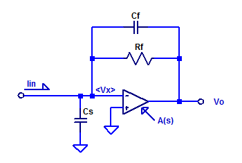
In this post, the current to voltage transfer function of a trans-impedance amplifier is derived. Consider a sample op-amp based trans-impedance amplifier as shown in the figure below.

Small-signal schematic of trans-impedance amplifier.

Capacitors \(C_f\) and \(C_s\) are included for completeness, as they do exist as parasitic elements in a real circuit. Parasitic shunt capacitance of \(R_f\) may be on the order of 100 fF. Capacitor \(C_s\) is the sum of routing capacitance (perhaps a few pF) and the input capacitance of the op-amp (perhaps 3 pF to 6 pF).

Continue reading “Trans-Impedance Amplifier – Transfer Function”

CD40106 Schmitt Trigger Relaxation Oscillator

In a traditional oscillator, oscillation is achieved by providing a loop-gain greater than unity and a phase-shift of \(0^o\) at some \(f_{osc}\). However, in the case of a relaxation oscillator, oscillation is achieved by switching between two discrete states. Often a relaxation oscillator is constructed with  a non-linear circuit element which can provide 2  threshold voltage levels to define two discrete states. One non-linear circuit element which is commonly employed in a relaxation oscillator is a schmitt trigger.

Due to the hysteresis developed internal to the schmitt trigger, two trigger thresholds are realized, namely \(V_N\) and \(V_P\). Where \(V_N\) is the negative threshold voltage and \(V_P\) is the positive threshold voltage. The hysteresis voltage is then,

$$ V_H = V_P – V_N $$

Ideally, the thresholds \(V_N\) and \(V_P\) would be centered around mid-supply (\(V_{dd}/2\)), however in practice this is only approximately true.

A minimal component count relaxation oscillator is shown in the figure below.

Schematic of CD40106 Schmitt-Trigger Relaxation Oscillator. Continue reading “CD40106 Schmitt Trigger Relaxation Oscillator”