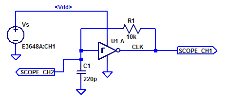
In this post the output drive characteristics of a Cd40106 are measured and analyzed. The drive strength of a gate is important in high-speed signaling in order to quickly charge/discharge PCB interconnect capacitance and the effective input capacitance of the receiving gates/ICs.
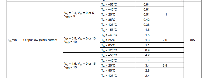
The datasheet’s specification for the CD40106’s output low current sink \(I_{OL}\) is shown in the figure below.

We can translate the typically sink current to an approximate resistance as,
$$ R_{OL,5} = \dfrac{V}{I} = {0.4}{0.001 } = 400 \; \Omega $$
From the datasheet we can calculated the typical output resistance for all 3 specified Vdd supply values as,
$$ R_{OL,5} = 400 \; \Omega \;\;\; R_{OL,10} = 192 \; \Omega \;\;\;R_{OL,15} = 221 \; \Omega $$
Note the output resistance is specified to be lower on a 10 V supply versus a 15 V supply. In the section below we will determine if indeed a 10 V supply yields the lowest output low resistance. Continue reading “CD40106 Output Drive Characteristics”
