In this post the output drive characteristics of a Cd40106 are measured and analyzed. The drive strength of a gate is important in high-speed signaling in order to quickly charge/discharge PCB interconnect capacitance and the effective input capacitance of the receiving gates/ICs.
The datasheet’s specification for the CD40106’s output low current sink \(I_{OL}\) is shown in the figure below.
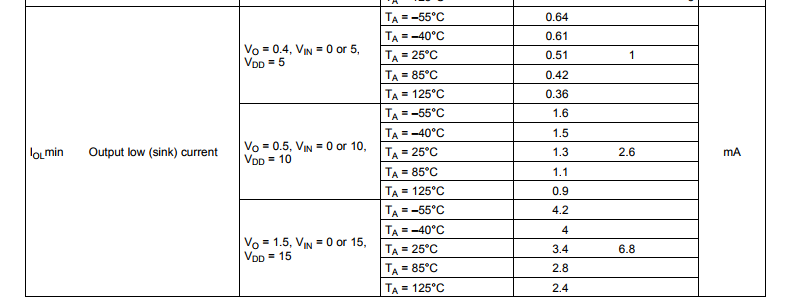
We can translate the typically sink current to an approximate resistance as,
$$ R_{OL,5} = \dfrac{V}{I} = {0.4}{0.001 } = 400 \; \Omega $$
From the datasheet we can calculated the typical output resistance for all 3 specified Vdd supply values as,
$$ R_{OL,5} = 400 \; \Omega \;\;\; R_{OL,10} = 192 \; \Omega \;\;\;R_{OL,15} = 221 \; \Omega $$
Note the output resistance is specified to be lower on a 10 V supply versus a 15 V supply. In the section below we will determine if indeed a 10 V supply yields the lowest output low resistance.
Measurement Setup
Each of the 6 gates internal to the Cd40106 are characterized separately and sequentially from gate A through to gate F. A schematic of the test setup is shown below.
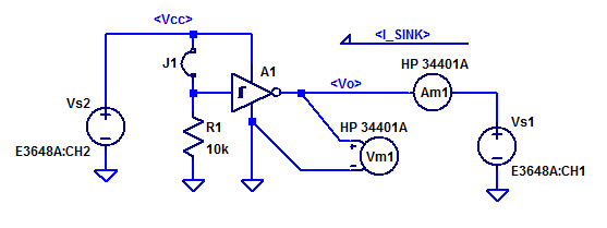
Bench supply \(V_{s2}\) provides the Vdd supply rail, which is programmaticly stepped from 3 VDC to 15 VDC. Resistor \(R_1\) is an input pull-down resistor which is included for each gate input (each gate has a separate resistor). Jumper \(J_1\) ( a mini-grabber test lead ) allows for the selection of an input logic high. Power supply \(V_{s1}\) is programmticly ramped from 0 VDC to Vdd in 100 mV increments. Ammeter \(A_{m1}\) measures the sink current into the gate-x output pin. Voltmeter \(V_{m1}\) measures the effective voltage at the gate output pin. Voltage sag due to interconnect wiring and burden voltage of \(A_{m1}\) are mitigated by connected the leads of \(V_{m1}\) directly to the GND and output pins of the Cd40106.
Physical construction is the same as the previous post Schmitt-Trigger Threshold Levels (CD40106). A photo of the DUT mounted to an FR4 test coupon is shown below.
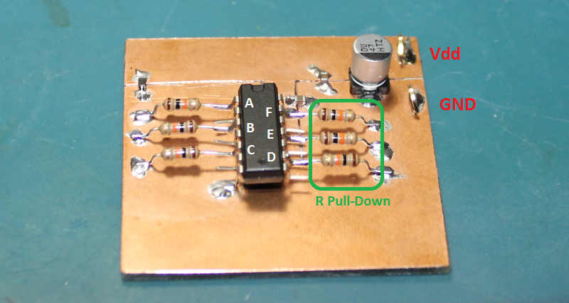
Note the ground pin is pin 7 of the 14-pin DIP package, which is located at the bottom left corner of the IC in the photo above.
Measurement Results
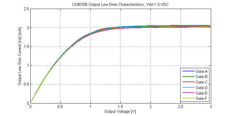
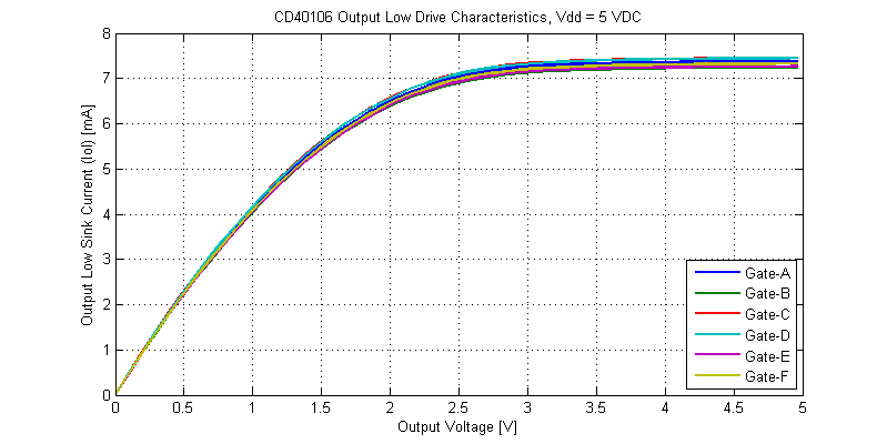
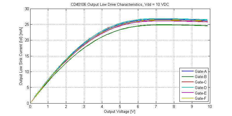
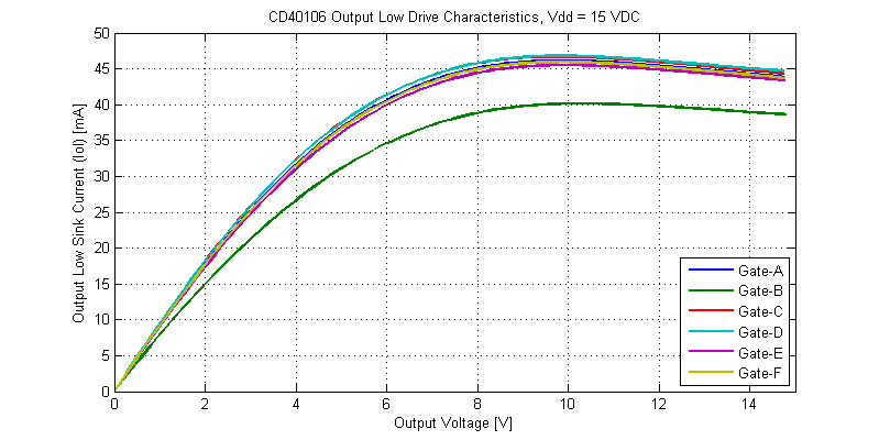
The output drive characteristics for an output low signal are shown in the figure below.
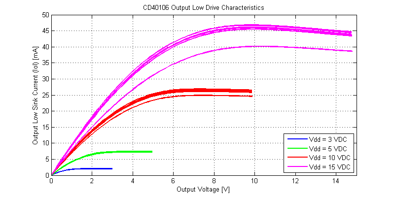
While the CD40106 is rated for operation at 3 VDC, even into a shorted load, the IC can sink a total of 2 mA per gate. When operated on a 15 VDC supply the CD40106 can sink a maximum of 45 mA with a shorted load to the Vdd supply rail. Interestingly, at elevated power dissipation levels the cd40106 folds-back in drive strength, this can be seen from the 10 V to 15 V region on the Vdd = 15V I-V sweeps.
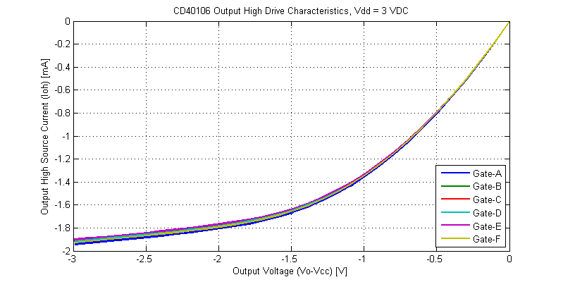
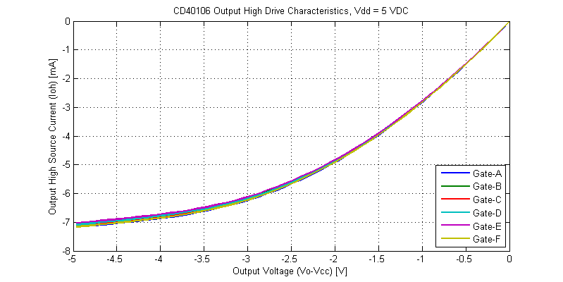
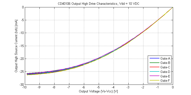
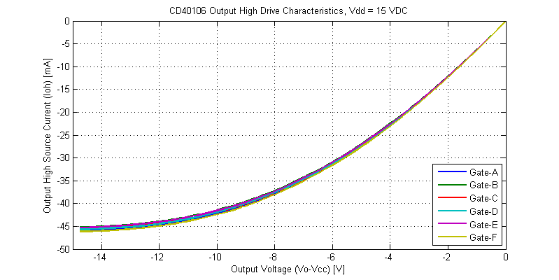
Output drive characteristics for an output-high signal are shown in the figure below.
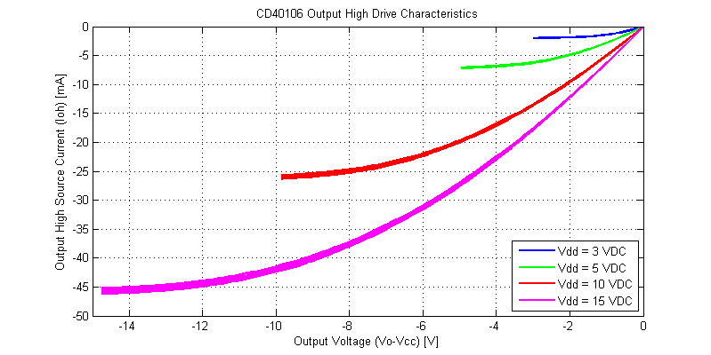
Comparing the output-high versus output-low I-V curves, there are a few subtle differences. The output-high drive characteristics are monotonic and do not appear to have any significant thermal-foldback. The initial slope of the output-high is steeper than that of the output-low state (higher output resistance). Both output high-low have similar peak drive currents into a shorted load.
We can estimated the instantaneous output resistance from the I-V curves collected above as,
$$ R_o = \dfrac{ \Delta V }{ \Delta I } $$
The output resistance of each gate versus load current is shown in the figure below.
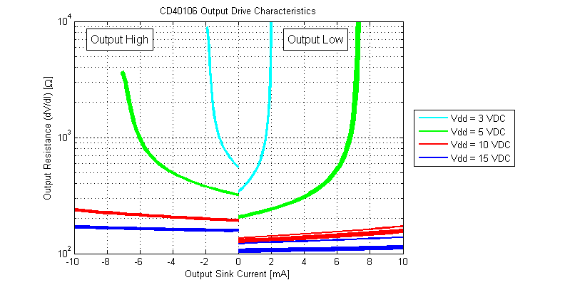
While the datasheet claims “Standardized, Symmetrical Output Characteristics”, in the figure above the output resistance for an output high is roughly 60% larger than that of an output low signal for the same magnitude of load current. The lowest output resistance of the CD40106 is achieved with logic output low at \(R_{OL} \simeq 110 \Omega\) with a 15 VDC supply.
The output resistance for all possible load currents is shown in the figure below.
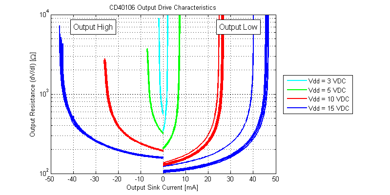
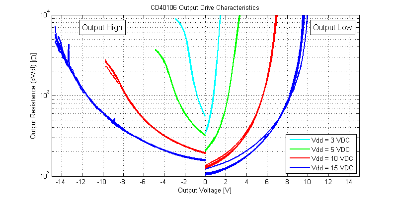
The output resistance of the CD40106 versus output voltage level is shown in the figure below.
Raw Data
The raw data for each of the 6 gates of the single Cd40106 tested, can be found as csv files below.
Output Low Drive Characteristics
– Iol @ 3 V
– Iol @ 5 V
– Iol @ 10 V
– Iol @ 15 V
Output High Drive Characteristics
– Ioh @ 3 V
– Ioh @ 5 V
– Ioh @ 10 V
– Ioh @ 15 V
Files are formatted as,
Va [V],..,Vf [V],Isinka [A],...,Isinkf [A]
Extras
Output Low Drive Strength
Output High Drive Strength
Hey, you may be interested in this model I created:
https://www.seventransistorlabs.com/Images/CD4001_TR.ckt
It uses this model,
https://people.rit.edu/lffeee/RIT_Models_For_LTSPICE.txt
although curiously I found it necessary to swap the NRD/NRS parameters for P/N to get the right characteristic.
The transistor model gives good enough agreement with a typical part (well within the spread of normal parts), and the ESD diodes are even modeled based on a real part.
Thanks for the link, it’s a good model. Perhaps conservative in regards to drive strength, but nothing wrong with that!