A schmitt-trigger to a first operates just like any digital buffer/inverter where a logic level input ( Gnd or Vdd ) yields some digital output value based on the logic function of the gate. What is different about an inverting schmitt-trigger over a basic inverter is the input threshold voltage changes depending on the gate’s output state. In the case of a schmitt-trigger the input threshold level receives a small positive feedback from the output. Hence when the output is triggered high, the input threshold voltage is boosted a small amount. Equivalently, when the output is low the input threshold voltage is lowered a small amount. This positive feedback of the output to the input is refereed to as hysteresis.
The transfers characteristics figure available from the CD40106 datasheet is shown below.
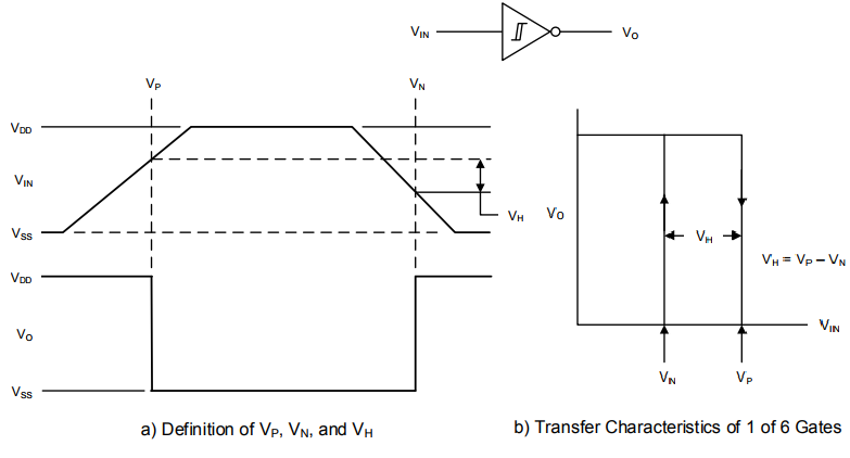
Note the 2 input threshold levels \(V_N\) and \(V_P\), where \(V_P\) is the input threshold required for the output to transition from high to low.
Measurement Setup
A schematic of the test setup is shown in the figure below.
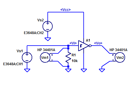
Power supply Vs2 (E3648A) is stepped from 3 VDC to 15 VDC programmaticly. Power supply Vs1 (E3648A) provides an input signal Vi to one gate of the CD40106. All gate inputs have 10 kOhm pull-down resistors. Voltmeter Vm1 (HP 34401A) samples the input signal Vi. Voltmeter Vm2 (HP 34401A) samples the output voltage Vo.
A typical bench power supply such as the E3648A used in this blog post, is single quadrant output. Meaning the supply can only source current for positive output voltage. Having no current sink capability means that the settling time for a new voltage set-point that is lower than the previous is very slow. As the supply relies on the LOAD and internal pull-down resistors to discharge the supplies output bypass capacitors. The addition of a 100 ohm pull down on the Vi signal line improves negative going settling times.
The precision of the E3648A on a 20V scale is approximately 1 mV. Hypothetically on could step the input Vi in 1 mV setup and wait for the output to transition to determine the threshold voltages. However, for the sake of test time the threshold voltages are determined by employing a modified binary search algorithm.
An alternate measurement scheme would be configure each gate as a very low-frequency relaxation oscillator (astable multivibrator) and measure the peak-peak voltage voltage on the integration capacitor. A multimeter configured for an measurement rate much greater than the oscillation frequency can be configured to measure MIN/MAX. The min result is Vtn and the max result is Vtp.
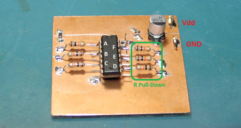
The DUT is mounted to FR4 blank coupon with a hand cut power plane. The input and output leads are raised above the ground plane for easy probe access. Each of the 6 gates in the CD40106 are instrumented by connecting mini-hook grabbers. A photo of the simple construction is shown in the figure below.
Measurement Results
The threshold voltages recorded for Gate-A of the CD40106 are shown in the figures below.
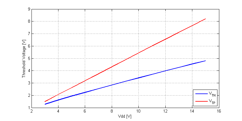
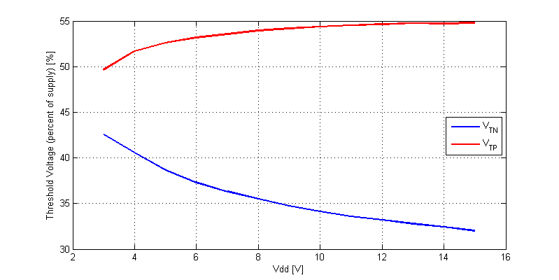
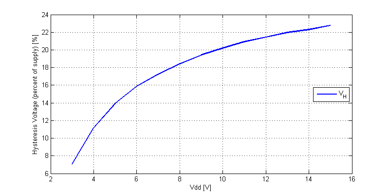
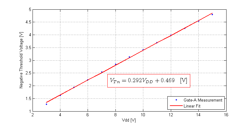
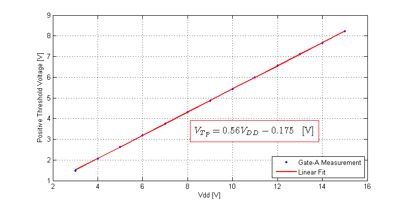
For brevity Input/Ouput plots for the remain 5 gates are omitted and instead a plot of threshold matching between all gates is included below.
Where the mismatch is defined as,
$$ V_{x,mismatch} = V_x – \text{AVG}( V_A, V_B,…,V_F ) $$
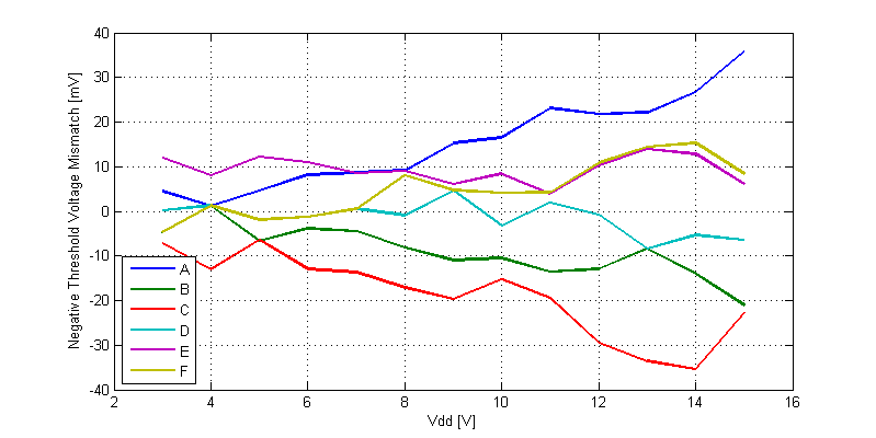
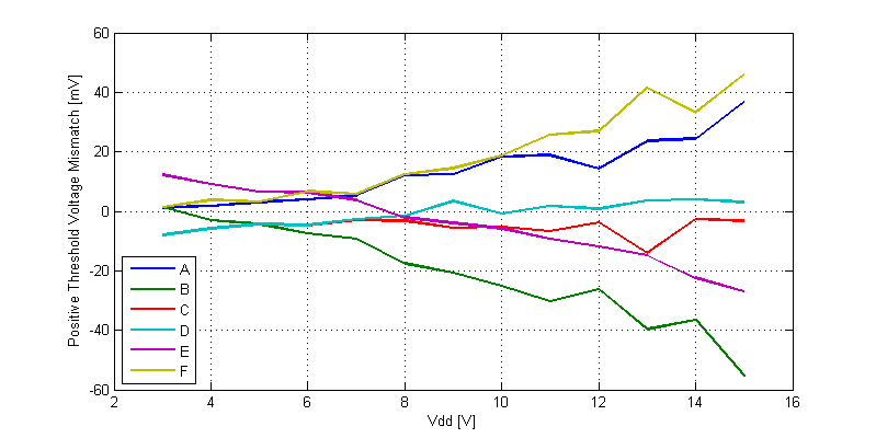
The matching between gates on a single CD40106 die at Vdd = 15 VDC is a span of \(\approx\) 100 mV, which is \(\pm\) 0.3 % of the supply value.
Raw Data
CD40106 Negative Threshold Voltages
CD40106 Positve Threshold Voltages
Files are formatted as,
Supply Voltage (Vdd) [V], VTx Gate-A [V],VTx Gate-B [V],...,VTx Gate-F [V]