In this blog post, the forward biased voltage-current relationship of a 1N4148 diode will be measured and analyzed.
Shockley in 1949, published a paper describing the behavior of a diode as,
$$ I_D = I_s \left( \exp \left( \dfrac{V_D}{\eta V_T}\right) -1 \right) $$
Where \( \eta \) is a constant representing the ideality of device, typical values of \( \eta \) range from 1 to 2 for silicon diodes.
$$ V_T = \dfrac{kT}{q} $$
At a room temperature of \(22\;^o\text{C}\) the thermal voltage is,
$$ V_T(22\;^o\text{C}) = \dfrac{(1.381\cdot 10^{-23})(273.15+22)}{1.602\cdot 10^{-19}} = 25.4 \text{ mV} $$
Measurement Setup
The lowest current measurement scale is 10 mA on a 34401A, so, for low current measurement a different approach is needed. For this blog post the forward I-V plot is divided into 2 regions. Test currents less than \(\approx 100\) uA will be measured using a low current setup. For test currents above 100 uA, the DCI measurement mode of a 34401 will be employed.
Low current
The DCI mode of a 34401A has a minimum scale of 10 mA. In order to measure nA to uA level test currents a 100 kOhm current shunt and voltmeter measures are employed. A schematic of the test setup is shown below.
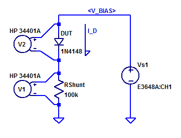
\(R_{shunt}\) and voltmeter \(V_1\) sample the DUT forward current \(I_D\) as,
$$ I_D = \dfrac{V_1}{R_{shunt}} $$
Voltmeter \(V_2\) samples the DUT’s forward voltage. Power supply \(V_{s1}\) is stepped programmatically from 0 to 10 V. The forward current at full output is then,
$$ I_D = \dfrac{V_{s1} – V_D}{R_{shunt}} \approx \dfrac{ 10 – 0.5 }{100\cdot 10^3} = 95 \;\;\; \text{[uA]} $$
Both voltmeters \(V_1\) and \(V_2\) are configured for Hi-Z input resistance. Note, this limits the maximum shunt to potential to 10 VDC, as 10V is the largest DCV measurement range supporting Hi-Z input resistance (100+ VDC measurement scales are 10 MegOhm input resistance only).
High Current
For test currents of 100 uA to 100’s of mA a textbook class topology is employed. A schematic of the test setup is shown below.
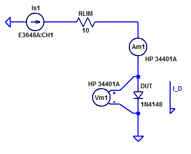
Bench power supply \(V_{s1}\) operates as current programmable current source. DUT test current is sampled via series ammeter \(A_{m1}\). DUT forward voltage is sampled by voltmeter \(V_{m1}\). Bench supply \(V_{s1}\) has a maximum output voltage of 20 VDC. All combination linear bench power supply with a constant voltage output have some output bypass/bulk capacitance between the output terminals. When the output capacitor is fully charged there is no current limiting its discharge rate (beyond the mechanics of the loading circuits). In order to protect the DUT from a high current discharge of the output bypass capacitors a series limiting resistor \(R_{lim}\) is employed. With the output at supply’s maximum output voltage, the peak discharge current while transitioning from contant-voltage to constant-current regulation is,
$$ I_{pk} = \dfrac{20-1}{10} = 1.9 \text{ [A]} $$
A 1N4148 is rated for a peak pulse current load of 2 A for a short duration.
Power dissipation of the DUT is important as to not overheat the semi-conductor junction, which will would eventually lead to some failure mode.
The power dissipation limit of the 1N4148 is shown in the datasheet excerpt below.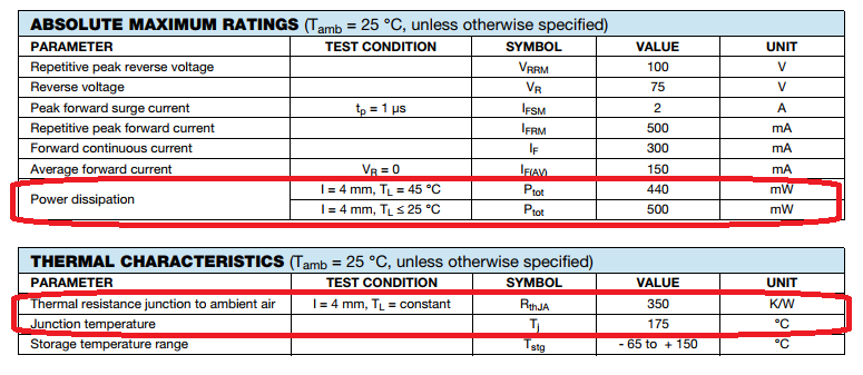
A 1N4148 is rated for a maximum power dissipation of 500 mW when mounted with 4 mm leads at 25 degC.
In the figure below the instantaneous IV curve with a constant power IV curve.
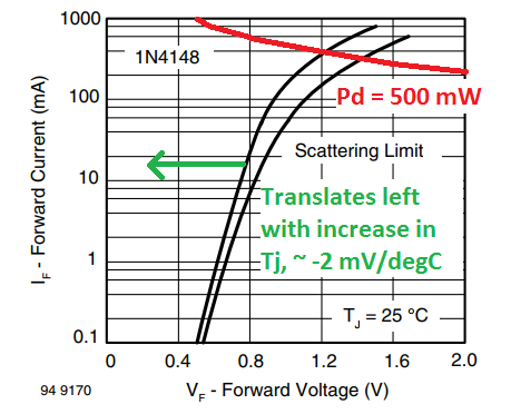
We can observe that if the junction temperature remains constant, the forward current at maximum Pd is between 250 mA to 300 mA. In reality for a static load test, the junction temperature will rise with power dissipation causing the forward voltage to decline. With a lower forward voltage and same current, less power is being dissipated by the DUT. We can expect the maximum power dissipation load point to be somewhere between 300 mA to 500 mA (when self-heating of the junction is considered).
The glass body of the diode has a length of 3.4 mm. A diagram of the package dimension is shown below.
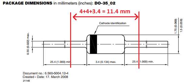
For easy of construction, the DUTs will be mounted axially without lead forming. Notching a slot of 11.4 mm width, yields a mounting arrangement with 4 mm lead length.
A photo of the DUTs mounted to the test-jig is shown below.
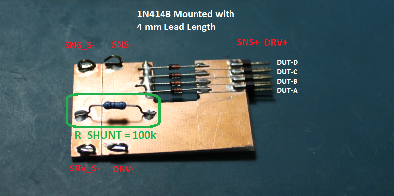
While the physical construction earns no beauty points, as will be seen below the DUTs follow the theoretical diode equation over 8 orders of magnitude (50 pA to 10’s of mA).
Measurement Results
Room temperature and the shunt resistor are recorded as,
$$\begin{matrix}
T_{amb}\; : & 21.1 \; ^oC \\
R_{Shunt}\;: & 100.48 \; k\Omega
\end{matrix}$$
The complete aggregate IV model (combining high and low sweeps) is shown in the figure below.
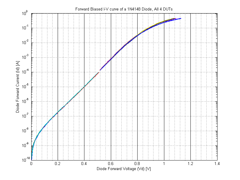
It is not obvious in the IV plot above that the low current curves don’t intersect high current curves. A plot showing the discontinuous region is shown below.
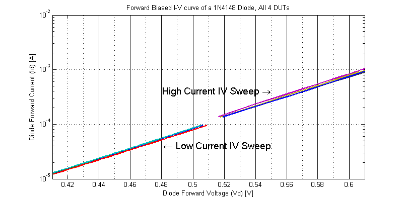
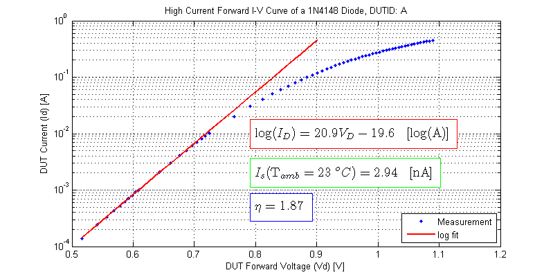
The rationale for this discontinuity is extremely important to appreciate. Note that the slope of the two segments are approximately equal. However the y-intercept of the log-line has changed. Between the two sweeps the ambient temperature had risen and trial runs of 500 mW power dissipation sweeps were conducted (raising the test-jig temperature above ambient). In fact, the saturation current \(I_s\) of a silicon diode roughly doubles for every +8 degC temperature rise. This is why it is customary to see the IV curve of a diode described as being instantaneous response or characterized via pulse measurement techniques. However the response shown above is still absolute, only it includes the thermal behavior of the device in addition to the IV relationship.
Low Current Model Fitting
For diode forwards voltages \(V_D\) greater than a few \(\eta V_T\) the exponential in the equation dominates and the equation can be simplified as
$$ I_D = I_s \left( \exp \left( \dfrac{V_D}{\eta V_T}\right) -1 \right) \approx I_s e^{ m V_D} $$
Where m is some constant.
\begin{align*} \log(I_D) &= \log(I_s e^{ V_D/(\eta V_T)} )\\ &=\dfrac{V_D}{\eta V_T} + \log(I_S)\end{align*}
Hence, we can fit the \(\log( I_D)\) to a first order function of the form,
$$ \log(I_D) = b_1 V_D + b_0 $$
Where the function coefficients equate to diode model parameters as,
$$ b_1 = \dfrac{1}{\eta V_T} $$
$$ \eta = \dfrac{1}{b_1 V_T} $$
$$ I_S = e^{b_0} $$
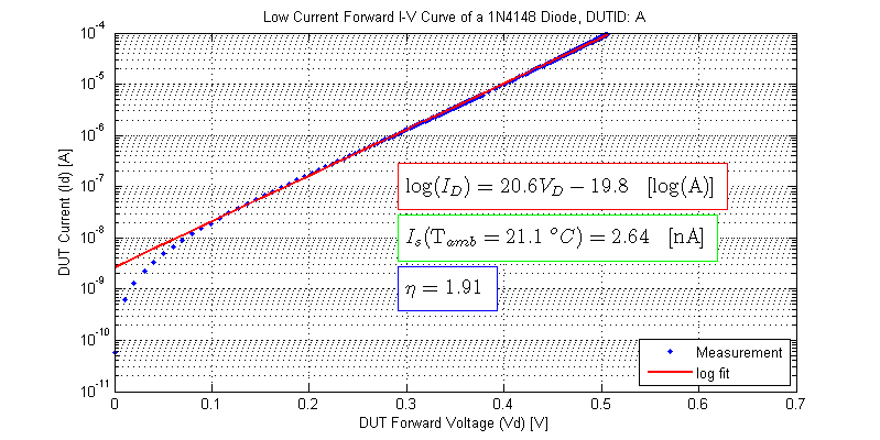
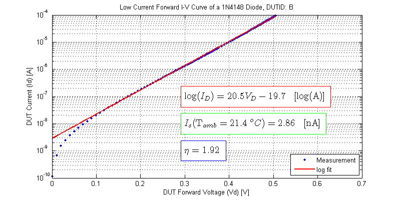
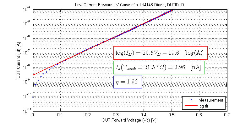
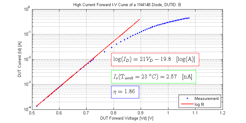
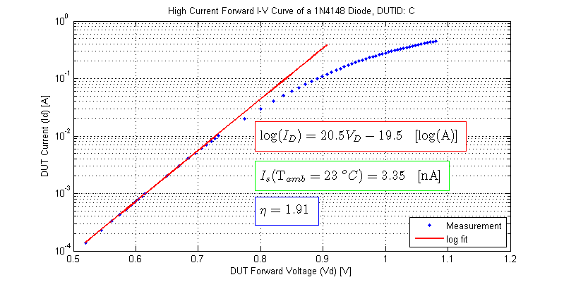
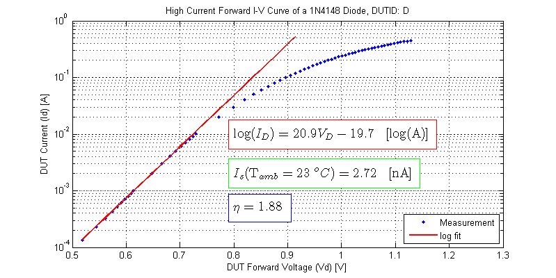
The results from fitting for each DUT to a log model are shown in the figures below.

High Current Model Fitting
Following the same procedure as outlined in the low current model fitting section, each DUT is fit to a log function. The data used for the log fit is DUT measurement points where \(V_D\) < 700 mV. The results from the model fitting are shown below.
High Current Dynamic Resistance
The small signal resistance of a diode can be found by linearizing the diode equation about a DC operating point as,
\begin{align*}
\dfrac{ \partial I_D}{ \partial V_D} &= \left(\dfrac{\partial}{\partial V_D}\right)I_s e^{ V_D/\eta V_T} \\
g_D &= \left(I_s e^{ V_D/\eta V_T} \right) \dfrac{1}{\eta V_T}
\end{align*}
Noting the factor of \(I_D\), the small-signal conductance becomes,
$$ g_D = \dfrac{I_D}{\eta V_T} $$
Equivalently, the small-signal resistance is the inverse of conductance as,
$$ r_D = \dfrac{\eta V_T}{I_D} $$
The theoretical dynamic resistance \(r_D\) and measured dynamic resistance are plotted in the figure below.
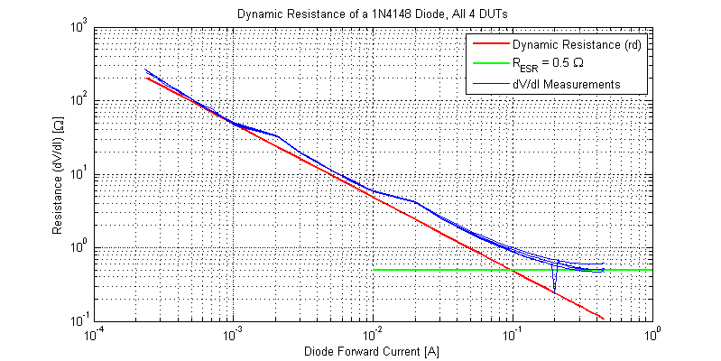
The first excursion in dynamic resistance at 1 mA, will need further investigation. The second excursion at 10 mA is due to range switching of the DMM. At low current the measured and theoretical dynamic resistance show reasonable agreement. At some point the effective small-signal resistance is dominated by the ESR of diode. The figure below plots the dynamic resistance of a 1N4148 near the constant resistance region.
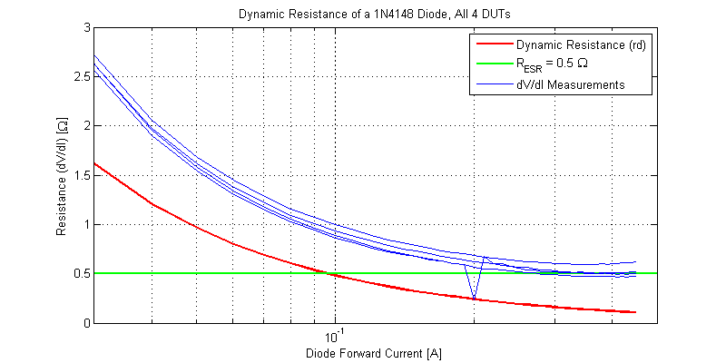
Between the glass body of the diode and sense measurement points the lead + jig resistance was measured to be \( \approx 5 m\Omega\) for each terminal, yielding a total ESR from mounting of 10 mOhms. The approximate 500 mOhms ESR is primarily due to the mechanics of the physical diode junction not the leads and test jig.
Low Current Model Agreement
The forward voltage where the current of a diode is equal to its saturation current can be solved as,
\begin{align*}
Id = I_s &= I_s\left( \exp\left((\dfrac{V_D}{\eta V_T} \right) – 1 \right) \\
1 &= \exp\left(\dfrac{V_D}{\eta V_T} \right) – 1 \\
2 &= \exp\left(\dfrac{V_D}{\eta V_T} \right) \\
\log(2) &= \dfrac{V_D}{\eta V_T}
\end{align*}
$$ V_D = \log(2)\eta V_T $$
Consider for example DUT-A, which would have a forward voltage of
$$ V_D(I_D=I_s) = (0.693)(1.91)(25.4 \;\text{mV}) = 33.6 \;\text{mV} $$
The figure below shows the IV behavior below 1 \(I_S \).
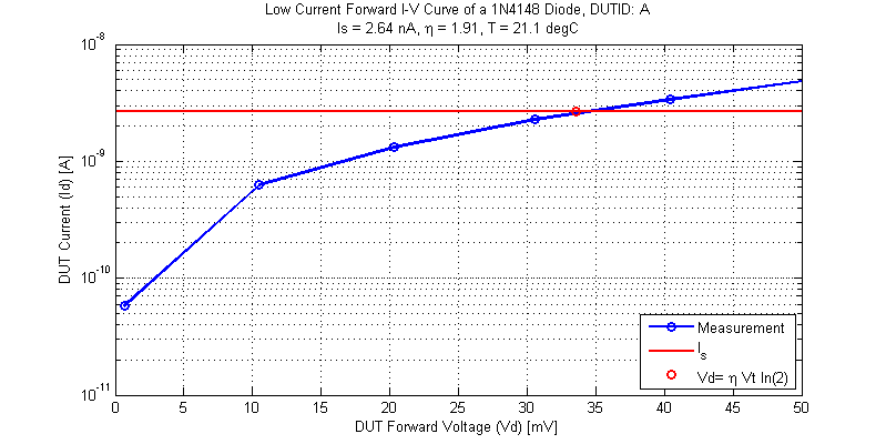
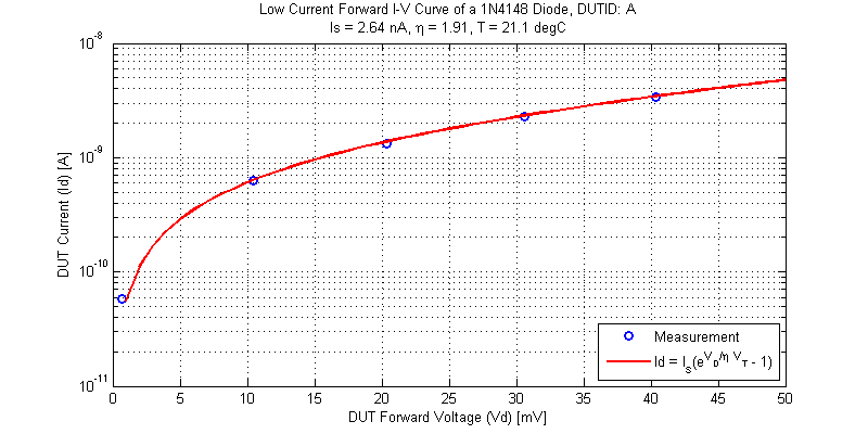
While the ‘-1’ term was committed for log model fitting, even at current levels where the ‘-1’ term is comparable to the exponential the measurements show good agreement. The figure below shows both the measurement data and the full diode model using the model parameters determined above.
Raw Data
The I-V curves collected for the 4 DUTs can be found as csv files below:
Low Current
– DUT A (\(T_{amb} = 21.1 \;^oC\))
– DUT B (\(T_{amb} = 21.4 \;^oC\))
– DUT C (\(T_{amb} = 21.5 \;^oC\))
– DUT D (\(T_{amb} = 21.5 \;^oC\))
High Current
– DUT A (\(T_{amb} = 23 \;^oC\))
– DUT B (\(T_{amb} = 23 \;^oC\))
– DUT C (\(T_{amb} = 23 \;^oC\))
– DUT D (\(T_{amb} = 23 \;^oC\))
Files are formatted as,
DUT Voltage [V], DUT Current [A]
Nice work. I was thinking of doing something similar since I couldn’t find a datasheet that showed the IV curve below 10uA.
One slight mistake I noticed is the temperature slope, which depends on current. At 0.1mA, -2mV/C is about right, but at 10mA, it’s closer to 1.5mV. Vishay’s datasheet shows this, as does a recent HackADay post:
https://hackaday.com/2018/04/16/two-cent-temperature-sensors/
In the diode equation ,for a 1n4148 , if Vf = 620 mV, Is = 7 nA you get a ridiculous value of 210A for If ?
I think I’ve got the arithmetic right?
That is for 25°C
Hello, I suspect you may have omitted the ideality factor in your diode equation. If I assume \(\eta = 1.9\), I would evaluate \(I_D\) as, $$ I_D = (7 \text{ nA})\exp\left( \dfrac{ 620 }{ 25.7 \cdot 1.9 }\right) \approx 2.3 \text{ mA} $$.
Hey, I’m a student and I’m struggling to find the forward bias dynamic resistance of this diode, any help?
Protect diodes against light – photo effect.
important link trustee wallet