When a silicon diode is sufficiently reverse biased, the junction undergoes either avalanche or zener breakdown. Zener breakdown is a quantum mechanical behavior which typically occurs at potentials less than -5 V or -6 V for silicon diodes. Avalanche breakdown occurs when a thermally generated electron-hole pair is sufficiently accelerated by the reverse bias electrical field, such that, when they impact a second carrier they cause impact ionization. These additional free carriers then cause more impact ionization and this becomes a multiplicative process. Ultimately conducting high levels of current due to the multiplicative gains of avalanche breakdown.
Breakdown specifications taken from the 1N4148 datasheet are shown highlighted in the figure below.
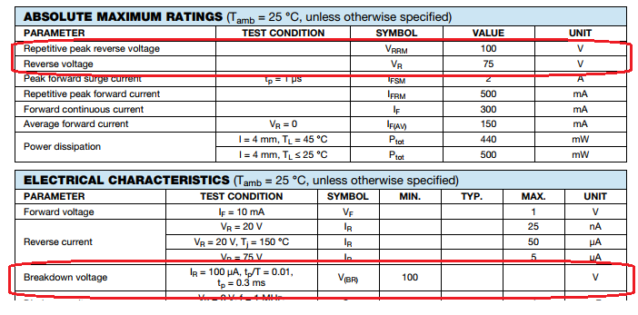
At room temperature, we expect to observe a breakdown voltage greater than 100 VDC. The recommended largest reverse working voltage is given as 75 VDC.
The standard spice model of a diode under reverse bias is the following,
\[
I_D =
\begin{cases}
I_s\left(e^{\eta qV_D/kT} -1 \right) + V_D\text{GMIN} &\quad\text{for} & -5\dfrac{\eta kT}{q} \leq V_D \leq 0 \\ \\
-I_s + V_D\text{GMIN} &\quad \text{for} & V_D < -5\dfrac{\eta kT}{q}\\ \\
-IBV & \quad \text{for} & V_D = -BV \\ \\
-I_S\left( e^{-q(BV+V_D)/kT}-1 + \dfrac{qBV}{kT}\right) & \quad \text{for} & V_D < – BV
\end{cases}
\]
Measurement Setup
Taking inspiration from the post, 1N4148 Reverse Bias Leakage Current a simillar approach is taken for instrumenting the nA level reverse bias currents. A 34401A samples a high resistance shunt, \(R_{shunt} = 1 M\Omega\).
With the breakdown voltage of a 1N4148 greater than 100 V, we will need to apply voltages bias voltages of at least 100 V. Having no programmable power supply capable of outputting over 100 V, a differen’t approach must be taken. Fortunately, most bench power supply have floating outputs and can be stacked. A total of 4 output channels were series stacked to obtain a peak output voltage of 122 VDC.
A schematic of the test setup is shown in the figure below.
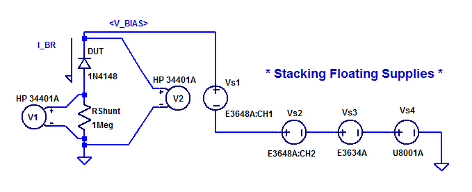
Here a 1 MOhm resistor is used as a current shunt resistor. Voltmeter V1 samples the potential across \(R_{shunt}\). Voltmeter V2 samples the bias potential being applied to the DUT. Power supplies Vs1, Vs2, Vs3, and Vs4 are series stacked to provide a maximum output of 122 VDC. Supply Vs3 was set for 31 VDC. Supply Vs4 was set for 51 VDC. Supplies Vs1 and Vs2 were stepped programmaticly from 0 to 20 VDC. Yielding a test voltage range of 82 VDC to 122 VDC.
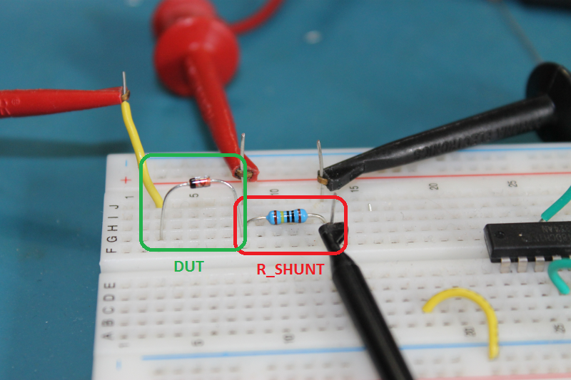
A photo of one DUT in the test setup is shown below.
Measurement Results
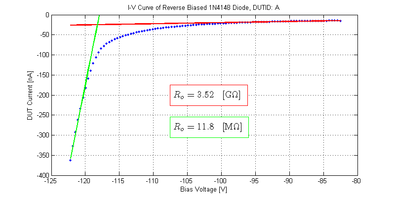
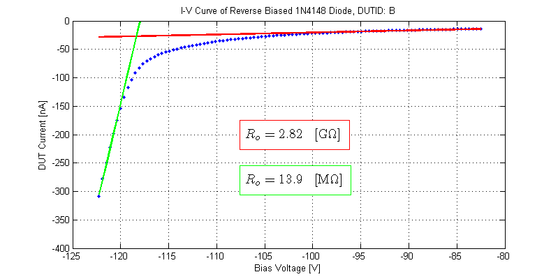
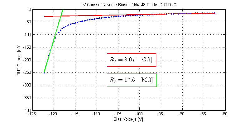
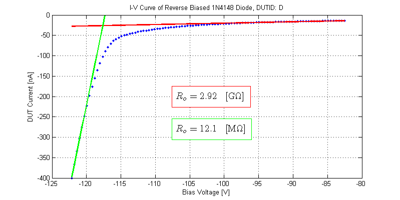
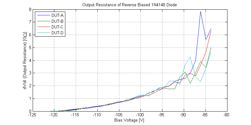
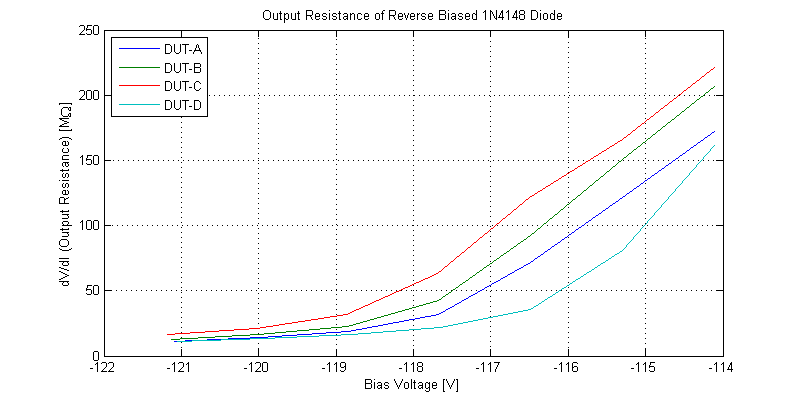
The I-V curve collected for each of the 4 DUTs is shown below.
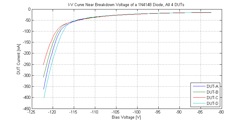
Before breakdown, at -100 VDC bias, the leakage of all 4 DUTs was approximately -20 nA. The breakdown knee voltage for all 4 DUTs was in the range of -117 VDC to -119 VDC.
The output resistance for of the 4 DUTs were estimated from the I-V curve. DUT-A demonstrated an output resistance of 11.8 MOhms just past the knee of breakdown. If sufficient bias voltage was available to measure the I-V curve into the uA’s of breakdown, the measured output resistance would be even lower.
Datasheet Specification
The typical reverse current characteristics provided in the 1N4148 datasheet are shown below. Augmented to the figure is a sketch of the approximate response obtained in measurements described above.
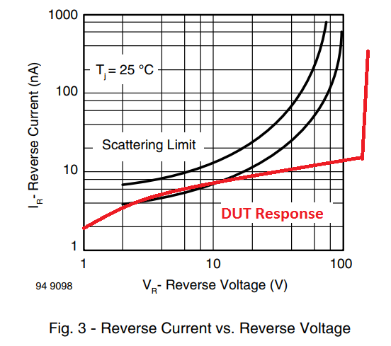
The behavior of the DUTs is significantly different for large reverse bias voltages.
Raw Data
The I-V curves collected for the 4 DUTs can be found as csv files below:
– DUT A
– DUT B
– DUT C
– DUT D
Files are formatted as,
DUT Voltage [V], DUT Current [A]