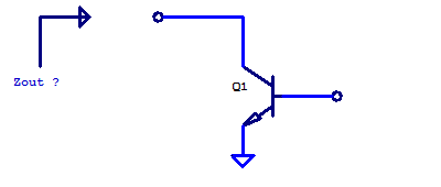
 In this post, a circuit equivalent model of the output impedance of a common-emitter amplifier will be developed. To begin, a low-frequency non-reactive model of the output resistance of a common-emitter (CE) amplifier will be solved. Proceeding models will include the capacitive elements of a CE amplifier. Separating the High-Frequency (HF) model into two distinct cases will allow for circuit analysis that is reasonable to perform by hand. The first HF model will be for when the base is ac-grounded and the emitter see a degeneration resistor. A second HF model is developed with a grounded emitter and with source resistance to the input (base) terminal. Concluding the post with a spice simulation to compare/validate the circuit equivalent models developed. The desired outcome of this post is to gain an intuition into what “it looks like” electrically speaking into the output of a CE amplifier.
Outline:
– Review of output resistance/impedance
– Low frequency model
– High Frequency Model – Grounded Base
– High Frequency Model – Grounded Emitter
– Spice Simulation
Review of Output Resistance/Impedance
From elementary circuit theory, one may recall that any linear circuit may be simplified about two arbitrary circuit nodes. One of the most common nodes to be chosen being the circuit common node (typically ground). With the second node to chosen as typically being an input or output node for single-ended circuits. In the case of differential circuits the simplification is made about the positive and negative branches of input/output ports. For any non-linear circuit such as a transistor amplifier, the non-linear behaviour can be linearized about an operating point for small signals. The figure below depicts this circuit simplification. Here some arbitrary Device Under Test (DUT) or Circuit Under Test (CUT) can be simplified into one of two basic circuits. On the left hand side, a voltage source with series resistance is refereed to as a Thévenin equivalent circuit. On the right hand side a current source shunted with a resistor is refereed to as a Norton equivalent circuit.
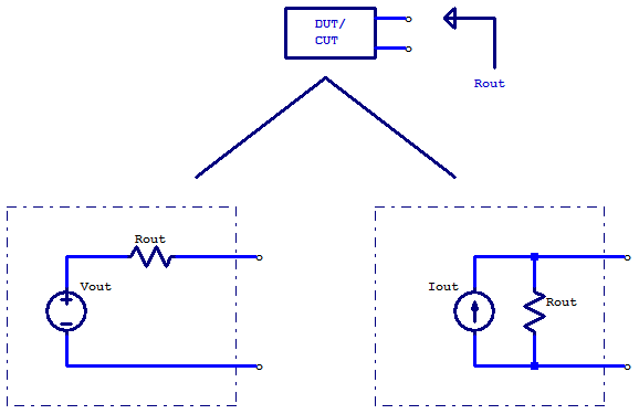
The choice of simplifying a circuit to either a Norton or Thévenin equivalent circuit is completely arbitrary, with the choice typically favouring the one which yields analytical convenience. Electrically looking into the terminals of either a Norton or Thévenin equivalent circuit, one could not distinguish between which style was chosen.
Electrical impedance (\(Z\)) can be applied equivalently to electrical resistance with the inclusion of a complex term \( X\) (reactance). For some specific frequency \( \omega = 2\pi f \), impedance is
\[ Z(\omega) = R + j X(\omega) \]
Impedance can be applied as a direct substitute for resistance, but the math must be done with complex arithmetic. It’s worth emphasizing here that reactance is orthogonal to resistance. When sinusoidally driven, at steady-state the reactive current is orthogonal to the source voltage and neither generates or expends any net energy.
Impedance can also be conveniently analyzed in the s-domain (frequency domain). A detailed explanation of the Laplace transform is beyond the scope of this blog, please consult an alternate reference on the use of the Laplace transform for circuits. An ideal capacitor has no series or parallel resistance and is exclusively a reactive element with reactance
\[ X_C = \frac{ -1 }{ \omega C} \]
its impedance is
\[ Z_C(\omega) = 0 + \frac{ 1 }{ j \omega C} \]
in the s-domain, its impedance is
\[ Z_C(s) |_{j\omega=s} = \frac{1}{sC} \]
A transistor is a non-linear circuit element, but can be linearized around an operating point. Take for example the circuit below, the base is biased with a constant current \( I_b\) and the collector is driven by a voltage source V1.
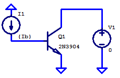
As a simulation example, the voltage source is swept from 0 VDC to 5 VDC. Collector current Ic is plotted on the figure below. During the first 200 mV of the sweep, the base-collector junction is strongly forward biased, resulting in the transistor being saturated. During saturation the collector current is a strong function of collector potential. The saturation region can be observed in the plot below, when the collector current ramps rapidly from 0 mA to 1.4 mA during the first 200 mV. This is analogous to a low output resistance, which can also be seen as the green trace in the plot.
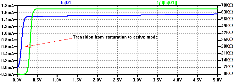
Once the base-collector junction is reverse biased the transistor is operating in the “active region”. As can be seen in the plot above from 500 mVDC to 5 VDC the collector current is a very weak function of collector potential. As the base-collector junction is increasingly reverse biased the depelation region expands, thereby narrowing the base charge region, resulting in base width modulation. As one may recall, current flows from the collector to the emitter in a transistor due to a minority concentration gradient across the base region. When the base charge is held constant and its width is narrowed the concentration gradient is increased, resulting in a larger collector current.
When a best fit line is fitted to the collector current in the active region as a function of collector potential, the x-axis intercept is refereed to as the early voltage. A sample spice simulation to illustrate the dependence of collector current Ic to collector potential Vce is shown in the two graphs below. Here an NPN transistor is biased with a current source to the base and a voltage source sweeps the collector potential, while recording collector current. The base current is incremented for each collector voltage sweep. On the left hand plot, all three of the best fit lines intercept the x-axis at approximately -100 V, for an early voltage of |100| V.
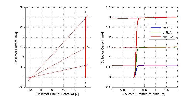
The equations for each of the best fit lines are the following
\begin{align*}
I_c \left( V_{CE} , I_b=2 \;\mathrm{\mu A}\right) &= 6\;\mathrm{\frac{\mu A}{V}} \cdot V_{CE} + 595 \; \mathrm{\mu A} \\
I_c \left( V_{CE} , I_b=5 \;\mathrm{\mu A}\right) &= 15\;\mathrm{\frac{\mu A}{V}} \cdot V_{CE} + 1484\; \mathrm{\mu A} \\
I_c \left( V_{CE} , I_b=10 \;\mathrm{\mu A}\right) &= 30\;\mathrm{\frac{\mu A}{V}} \cdot V_{CE} + 2957\; \mathrm{\mu A}
\end{align*}
What’s important to take away from this, is that collector current has a voltage dependence of approximately \( 1/V_A\). For the simulation example above, this is a voltage coefficient of \( 1 \% / V \) . Consequently, the relation of current flow to applied voltage is conductance and its inverse is resistance. Thereby allowing the voltage coefficient of collector current to be modelled as an output resistance about a DC operating point for collector current.
\[ r_o = \frac{ 1 }{ I_C \cdot 1/V_A} = \frac{V_A}{I_C} \]
A modified small signal model of an NPN transistor is shown below. This model is refereed to as the hybrid-\(\pi\) model. An entire blog post could be devoted to its derivation, and will not be covered in this post. The model below is a simplification of the full hybrid-\(\pi\) model. In the full model all device terminals would have series resistance and inductance. For the collector and emitter terminals the series resistance is an order of magnitude lower than that of the equivalent series resistance to the base terminal. In all future blog posts, collector and emitter series interconnect parasitics will be omitted.

For this blog, the elements of the hybrid-\(\pi\) model are the following:
\[ g_m = \frac{ Ic }{ V_{thermal} } \]
\[ R_b = \rm{constant} = 0 \]
\[ C_\pi = C_{be,d} + C_{be,j} \simeq C_{be,0}\sqrt{2} + g_m \tau_f \]
\[ r_\pi = \frac{\beta}{g_m} \]
\[ C_{\mu} = C_{bc,0} \sqrt{2} \]
To apply the hybrid-\(\pi\) model to a basic CE amplifier, all circuit elements must be substituted with their small-signal equivalent. The emitter terminal is tied to a common potential or an ac-ground. If the source element to the input of the CE amplifier is voltage source, then it is “ac-shorted” leaving only its series source resistance to ac-ground. In the case of a current source driving the input of a CE amplifier, the current source is “opened”, leaving only its shunted output resistance. A small signal circuit of a CE amplifier with the capacitive elements omitted is shown in the figure below

For the simplest case of having the emitter tied directly to ground, no voltage can ever developed across \( r_\pi \). Resulting in an output resistance that always equals the transistors intrinsic output resistance \(r_o\), regardless of the magnitude of \( R_S \). Note that an extremely large source resistance is nothing more than an idealized current source.
Low Frequency – (non-reactive model)
For low frequency (LF) small signals the hybrid-pi model can be simplified to include only non-reactive elements (i.e. no inductors or capacitors). With the parasitic capacitance across the base-emitter and base-collector junctions, as well as the dynamic base-emitter capacitance removed, the resulting small signal circuit is shown in the figure below. To analytically determine the output resistance (not impedance since reactive elements are excluded), we may either apply a test voltage or test current to the output and solve for the corresponding current or voltage respectively. The choice of applying a test voltage versus a test current is agnostic. For this circuit a test current is advantageous since the total current through both the dependent current source \( g_m V_\pi\) and \(r_o\) must equal the applied test current. At the emitter node, the entering current \(I_T\) will divide between \(r_\pi\) and \(R_E\) as a current divider. Allowing for an easy solution of \(V_\pi\) as a function of \(I_T\).
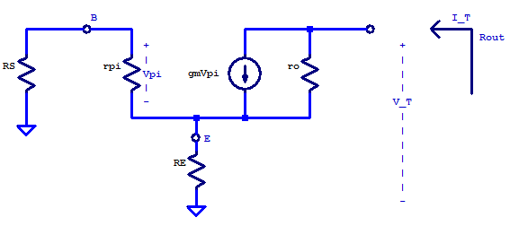
To begin we establish that the test current \( I_T\) will enter the collector terminal and the resulting test voltage \(V_T\) is developed with respect to the small-signal ground. Since the collector of the small-signal model only has connectivity with the emitter terminal, the current entering the emitter node must equal the current leaving the collector node. Current through the resistor \(r_\pi\) can be solved as a current divider
\[ I_{r_\pi} = \frac{I_T R_E}{R_E + r_\pi + R_S} \]
Noting that circuit potential \(V_\pi\) is referenced as positive at the base node and negative at the emitter node
\[ V_\pi = -r_\pi I_{r_\pi} \]
Substitution of \(I_{r_\pi}\) yields
\[ V_\pi = \frac{- r_\pi R_E}{R_E + r_\pi + R_S} I_T \]
Emitter potential \(V_E\) is the current divided into \(R_E\) multiplied by \(R_E\), which is the following
\[ V_E = \frac{R_E \left( r_\pi + R_S \right)}{ R_E + r_\pi + R_S }I_T \]
Finally the test voltage \(V_T\) must be equal the potential developed across \( R_E\) and \( r_0 \)
\[ V_T = V_E + \left( I_T – g_m V_\pi \right) r_o \]
\[ V_T = \frac{R_E \left( r_\pi + R_S \right)}{ R_E + r_\pi + R_S } I_T + r_o I_T + \frac{g_m r_o r_\pi R_E}{R_E + r_\pi + R_S} I_T \]
The output resistance is then simply
\[ R_{out} = \frac{V_T}{I_T} \]
\begin{equation}
R_{out} = \frac{R_E \left( r_\pi + R_S \right)}{ R_E + r_\pi + R_S } + \left[ 1 + \beta\frac{R_E}{R_S + r_\pi + R_E}\right] r_o \tag{LF.1}\label{LF.1}
\end{equation}
What’s important to acknowledge here is that when \(R_E\) is large and \(R_S\) is small any incremental change in test current is shunted across \(r_\pi\). Which in response drives an additional \(\beta\) times the incremental current across \(r_o\). Resulting in an output resistance which appears \( \beta \) times larger than the intrinsic output resistance \( r_o\).
When \(R_S >> \{ R_E, r_\pi \}\) then
\[ R_{out} \simeq R_E + r_o \]
If \( R_E >> r_\pi \) and \( R_S << r_\pi \)
\begin{align*}
R_{out} &= r_\pi + \left[ 1 + \beta \right] r_o \\
R_{out} &\simeq \beta r_o
\end{align*}
Circuit Equivalent Model
From equation (\ref{LF.1}) a circuit equivalent model can be constructed as a series string of three resistors. Beginning with the first resistor as the parallel combination of \( R_E || \left( r_\pi + R_s \right) \). A second resistor equal to the intrinsic output resistance \( r_o \). Thirdly a feedback induced resistor \( R_{fo} \). Below is a schematic representation of the circuit equivalent model.
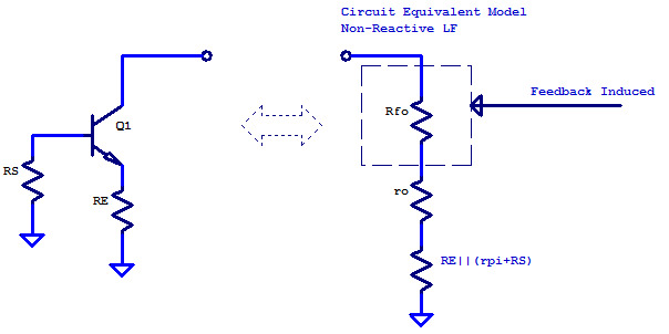
Equating the output resistance of the circuit equivalent model to (LF.1), the value of \(R_{fo}\) may be determined.
\begin{align*}
R_{out} &= R_E||\left(r_\pi + R_S\right) + r_o + R_{fo} \\
R_{out} &= \frac{R_E \left( r_\pi + R_S \right)}{ R_E + r_\pi + R_S } + \left[ 1 + \beta\frac{R_E}{R_S + r_\pi + R_E}\right] r_o \\ \\
R_{fo} = \beta \frac{R_E}{R_S + r_\pi + R_E}
\end{align*}
Grounded Emitter – High Frequency
Including capacitive elements \( C_\pi \) and \( C_\mu \), there now exists an AC feedback from the output terminal to the input terminal through \( C_\mu \). Contrary to the non-reactive model previously developed, with the emitter grounded the output feeds back to the input terminal. A small-signal model of the grounded-emitter CE amplifier is shown below
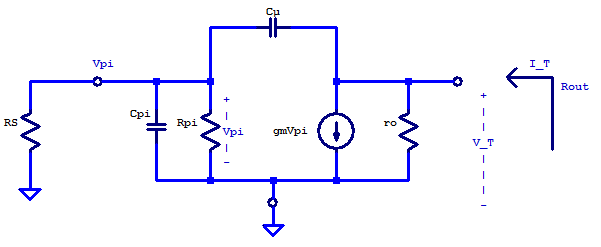
To solve for the output impedance, a test current \( I_T \) is applied to the output terminal of the CE amplifier. Applying KCL at the \( V_T \) node yields
\[ \frac{V_T}{r_o} + g_mV_\pi + \left( V_T – V_\pi \right)sC_\mu = I_T \tag{GE.1}\]
Applying KCL at the \( V_\pi \) node yields
\[ \frac{V_\pi}{R_S} + \frac{V_\pi}{r_\pi} + V_\pi s C_\pi + \left( V_\pi – V_T \right)sC_\mu = 0 \tag{GE.2} \]
Simplifying (GE.2)
\[ V_T s C_\mu = V_\pi \left( \frac{1}{R_S} + \frac{1}{r_\pi} + sC_\pi + sC_\mu \right) \tag{GE.3}\]
\[ V_T = V_\pi \left( \dfrac{r_\pi + R_S + sr_\pi R_S\left( C_\pi + C_\mu \right)}{sR_Sr_\pi C_\mu} \right) \tag{GE.4}\]
Simplifying (GE.1)
\[ V_T \left( \frac{1}{r_o} + sC_\mu \right) + V_\pi \left( g_m – sC_\mu \right) = I_T \tag{GE.5}\]
\[ V_\pi = \dfrac{I_T – V_T \left( \frac{1 + s r_o C_\mu}{r_o} \right) }{g_m – s C_\mu} \tag{GE.6}\]
Substitution of (GE.6) into (GE.4) yields
\[ V_T = \left( \dfrac{I_T – V_T \left( \frac{1 + s r_o C_\mu}{r_o} \right) }{g_m – s C_\mu} \right) \left( \dfrac{r_\pi + R_S + sr_\pi R_S\left( C_\pi + C_\mu \right)}{sR_Sr_\pi C_\mu} \right) \tag{GE.7} \]
Solving for \(V_T\)
\[ V_T \left[ 1 + \dfrac{ \left( \frac{1 + s r_o C_\mu}{r_o} \right)\left( r_\pi + R_S + sr_\pi R_S\left( C_\pi + C_\mu \right) \right) }{ \left(g_m – s C_\mu\right) \left( sR_Sr_\pi C_\mu \right) } \right] = \dfrac{ r_\pi + R_S + sr_\pi R_S\left( C_\pi + C_\mu \right) }{\left(g_m – s C_\mu\right) \left( sR_Sr_\pi C_\mu \right) } \tag{GE.8}\]
\[ V_T = \dfrac{ r_\pi + R_S + sr_\pi R_S\left( C_\pi + C_\mu \right)}{\left(g_m – s C_\mu\right) \left( sR_Sr_\pi C_\mu \right) + \left( \frac{1 + s r_o C_\mu}{r_o} \right)\left( r_\pi + R_S + sr_\pi R_S\left( C_\pi + C_\mu \right) \right) } I_T \tag{GE.9} \]
The output impedance is then
\[ Z_{out} (s)= \dfrac{ r_\pi + R_S + sr_\pi R_S\left( C_\pi + C_\mu \right)}{ \frac{r_\pi + R_S }{r_o} + s g_m R_S r_\pi C_\mu + s \frac{r_\pi R_S\left( C_\pi + C_\mu \right)}{r_o} + sC_\mu \left( r_\pi + R_S \right) + s^2 r_\pi R_S \left( C_\pi + C_\mu \right)C_\mu – s^2 R_S r_\pi C_\mu^2} \tag{GE.10}\label{GE.10} \]
At present Equation (GE.10) is not overly insightful (at all). To gain a greater insight into the behaviour of (GE.10) as a function of frequency, we will solve for the approximate poles and zeros of Z(s). For clarity, rewriting Z(s) as a general function with a first order numerator and second order denominator yields
\begin{equation}
Z_{out}(s) = \dfrac{ a_0 + a_1s }{ b_0 + b_1s + b_2 s^2 } \tag{GE.11}
\end{equation}
Where the \( a_n \) and \( b_n \) coefficients are the following
\begin{align*}
a_0 &= r_\pi + R_S \\
a_1 &= r_\pi R_S\left( C_\pi + C_\mu \right)\\
b_0 &= \frac{r_\pi + R_S }{r_o} \\
b_1 &= g_m R_S r_\pi C_\mu + \frac{r_\pi R_S\left( C_\pi + C_\mu \right)}{r_o} + C_\mu \left( r_\pi + R_S \right) \\ \\
b_2 &= r_\pi R_S \left( C_\pi + C_\mu \right)C_\mu – R_S r_\pi C_\mu^2\\
b_2 &= r_\pi R_S C_\pi C_\mu
\end{align*}
The zero (root of the numerator) occurs at
\begin{align*}
z_1 &= \dfrac{-a_0}{a_1} = \dfrac{-\left( r_\pi + R_S \right)}{ r_\pi R_S\left( C_\pi + C_\mu \right)}\\
z_1 &\simeq \dfrac{-\left( r_\pi + R_S \right)}{ r_\pi R_S C_\pi }
\end{align*}
To solve for the poles of Z(s), we could attempt to: factor the denominator, apply the quadratic equation, or assume the two poles are well separated. If we assume the poles are well separated then the denominator D(s) can be approximated as
\begin{align*}
D(s) &= b_0 + b_1 s + b_2 s^2 \\
&= b_0 \left( 1 + \frac{b_1}{b_0} s + \frac{b_2}{b_0}s^2 \right) \\
&= b_0 \left( 1 – \frac{s}{p_1} \right)\left( 1 – \frac{s}{p_2} \right)
\end{align*}
Since we assumed the poles are well separated, the dominant pole (lowest in frequency), dominates the inverse addition will the second pole. The approximate solution of the poles is then
\begin{align*}
\left( 1 – \frac{s}{p_1} \right)\left( 1 – \frac{s}{p_2} \right) &= 1 – \frac{s}{p_1} – \frac{s}{p_2} + \frac{s^2}{p_1 p_2} \\
&\simeq 1 – \frac{s}{p_1} + \frac{s^2}{p_1 p_2}\\ \\
p_1 &= \;- \dfrac{b_0}{b_1} \tag{GE.12} \\ \\
p_2 &= \dfrac{b_0}{b_2 p_1} \tag{GE.13}
\end{align*}
The dominant pole \(p_1\) of \( Z(s) \) is
\begin{align*}
p_1 &\simeq – \dfrac{b_0}{b_1}\\
p_1 &= \left(\dfrac{-1}{g_m R_S r_\pi C_\mu + \frac{r_\pi R_S\left( C_\pi + C_\mu \right)}{r_o} + C_\mu \left( r_\pi + R_S \right)}\right)\left( \dfrac{r_\pi + R_S}{r_o}\right) \\
p_1 &=\dfrac{-\left(r_\pi + R_S \right)}{g_m R_S r_\pi r_o C_\mu}
\end{align*}
The second pole \( p_2 \) is
\begin{align*}
p_2 &\simeq \dfrac{b_0}{b_2 p_1} \\
p_2 &= \dfrac{\left(-g_m R_S r_\pi r_o C_\mu\right)\left( r_\pi + R_S\right) }{\left( r_\pi + R_S\right) r_o r_\pi C_\mu C_\pi} \\
p_2 &= \dfrac{-g_m}{C_\pi}
\end{align*}
When \(Rs << r_\pi\), the poles and zeros are the following
\begin{align*}
z_1 &= \dfrac{-a_0}{a_1} = \dfrac{-\left( r_\pi + R_S \right)}{ r_\pi R_S\left( C_\pi + C_\mu \right)}\\
z_1 &\simeq – \dfrac{1}{ R_S C_\pi }
\end{align*}
The dominant pole \(p_1\) of \( Z(s) \) is
\begin{align*}
p_1 &\simeq – \dfrac{b_0}{b_1}\\
p_1 &= \dfrac{-1}{g_m R_S r_\pi C_\mu + \frac{r_\pi R_S\left( C_\pi + C_\mu \right)}{r_o} + C_\mu \left( r_\pi + R_S \right)} \dfrac{r_\pi + R_S}{r_o} \\
p_1 &= – \dfrac{1}{ r_o C_\mu}
\end{align*}
The second pole \( p_2 \) is
\begin{align*}
p_2 &\simeq \dfrac{b_0}{b_2 p_1} \\
p_2 &= \dfrac{\left(-roC_\mu \right)\left( r_\pi + R_S\right) }{ \left(r_\pi R_SC_\pi C_\mu \right) r_o} \\
p_2 &= – \dfrac{1}{R_SC_\pi}
\end{align*}
When the source resistance is low compared to \( r_\pi \), \( Z(s) \) is approximately a single pole function. Since \( p_2 \simeq z_1 \), pole \( p_2 \) “cancels” zero \( z_1 \), leaving only the dominant pole \( p_1 \). The output then appears as just the intrinsic elements \(ro\) and \( c_\mu \) in parallel to ground.
Circuit Equivalent Model
To develop a circuit equivalent model for Equation (\ref{GE.10}) we begin with just the intrinsic elements \( r_o\) and \( C_\mu \) in parallel. To add an additional pole and zero, a series resistor and capacitor are added in parallel to the intrinsic elements. A schematic of the circuit equivalent model is the following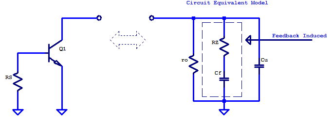
The two poles created are
\[ p_a = \frac{-1}{r_o \left( C_f + C_\mu \right)} \;\;\;\;\; p_b = \frac{-1}{R_Z C_\mu } \]
Assuming \( C_f >> C_\mu \) then pole \( p_a \) becomes
\[ p_a = \frac{-1}{r_o C_f } \]
Equating pole \( p_a \) to pole \( p_1 \) of \(Z(s)\) and solving for equivalent circuit element \( C_f \)
\begin{align*}
\frac{1}{r_o C_f } &= \dfrac{-\left(r_\pi + R_S \right)}{g_m R_S r_\pi r_o C_\mu} \\\\
C_f &= \left(\dfrac{R_S}{r_\pi + R_S} \right) \beta C_\mu
\end{align*}
For the circuit equivalent model, a zero is created at
\[ z_a = \frac{-1}{ R_z C_f } \]
Equating zero \( z_a \) to zero \( z_1 \) of \(Z(s)\) and solving for equivalent circuit element \( R_z \)
\begin{align*}
\frac{-1}{ R_z C_f } &= \dfrac{-\left( r_\pi + R_S \right)}{ r_\pi R_S C_\pi } \\
R_z &= \dfrac{ r_\pi R_S C_\pi }{\left( r_\pi + R_S \right)} \left(\dfrac{r_\pi + R_S }{R_S \beta C_\mu} \right) \\
R_z &= \left( \dfrac{C_\pi}{C_\mu } \right) \dfrac{1}{g_m} \\
\end{align*}
When the transistor is biased for large collector currents, \( C_\pi \simeq g_m \tau_f\), resulting in the circuit equivalent parameter \( R_z \) approaching a device specific constant of
\[R_z = \left( \dfrac{\tau_f}{C_\mu } \right) \]
When Rs is large then
\[ C_f \simeq \beta C_\mu \]
When \(R_S << r_\pi\) the circuit equivalent model simplifies to just the intrinsic elements \(r_o\) and \(C_\mu\)
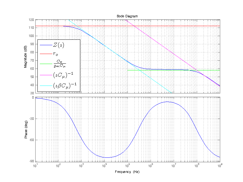
Comparing the circuit equivalent model to output impedance \( Z(s) \) can be illustrated with the use of a bode plot of \(Z(s)\). A bode plot for large source resistance is shown in the figure below. The impedance of the intrinsic elements \( r_o \) and \( c_\mu\) are included, in addition to the two circuit equivalent elements \(R_z\) (plotted in green) and \(C_f\) (plotted in cyan). Two poles and one zero are visible for \(Z(s)\), as calculated above. As the source resistance increases, the pole and zero on the cyan trace are pushed lower in frequency. The pole and zero translate at most by a factor of \( 1/ \beta \) (approximately two decades).
Grounded Base – High Frequency
With the base terminal tied to grounded, the feedback path from the output to input occurs by sampling the output current through resistor \(R_E\) and generating series potential with respect to the input. To solve for the output impedance of a CE amplifier being driven by a low-resistance source (ac-grounded base), we could first simplify the small-signal schematic as two independent circuits. Capacitor \( C_\mu \) in the hybrid-\(\pi\) model could be separated into a second circuit, to ultimately be recombined later. As \(C_\mu\) has no impact on the feedback path of the amplifier.
Since a general equation of \( Z(s) \) is desired to compare against a spice simulation, \( C_\mu\) is included from the beginning of the analysis (honest answer: did not think of it while handwriting the outline of the post). Establishing the relation of test current \( I_T \) and test voltage \( V_T \) can be seen on the small-signal schematic below
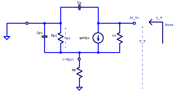
Applying KCL to the \( V_T \) node yields
\[ \dfrac{V_T – (-V_\pi)}{r_o} + g_mV_\pi + V_T s C_\mu = I_T \tag{GB.1} \]
Applying KCL to the \( -V_\pi \) node yields
\[ \dfrac{(-V_\pi)}{R_E} + \dfrac{(-V_\pi)}{r_\pi} + (-V_\pi)sC_\pi – g_mV_\pi + \dfrac{(-V_\pi) – V_T}{r_o} = 0 \tag{GB.2}\]
Collecting terms of (GB.1)
\[ V_T \left( \frac{1}{r_o} + sC_\mu \right) + V_\pi \left( \frac{1}{r_o} + g_m \right) = I_T \tag{GB.3}\]
Collecting terms of (GB.2)
\[ V_T\left( \frac{-1}{r_o} \right) + V_\pi \left( – \frac{1}{R_E} – \frac{1}{r_\pi} – sC_\pi – g_m – \frac{1}{r_o} \right) = 0 \tag{GB.4}\]
Solving for \( V_\pi \) of (GB.3)
\[ V_\pi = \dfrac{I_T – V_T \left( \frac{1}{r_o} + s C_\mu \right) }{\frac{1}{r_o} + g_m} \tag{GB.5}\]
\[ V_\pi = \dfrac{I_T}{g_m} – V_T\dfrac{ \left( \frac{1}{r_o} + s C_\mu \right) }{ g_m} \tag{GB.6} \]
Substitution of (GB.6) into (GB.4)
\[\frac{V_T}{r_o} + \left[ \dfrac{I_T}{g_m} – V_T\dfrac{ \left( \frac{1}{r_o} + s C_\mu \right) }{ g_m}\right] \left[ \frac{r_\pi r_o + R_E r_o + R_E r_\pi + R_E r_\pi r_o\left( sC_\pi + g_m\right)}{R_E r_\pi r_o}\right] = 0 \tag{GB.7}\]
Expanding and collecting terms
\[ V_T \left[ … \right] = – \frac{I_T}{g_m} \left[ … \right] \]
\[ V_T = \frac{I_T}{g_m} \left[ \dfrac{ \left(r_\pi r_o + R_E r_o + R_E r_\pi + R_E r_\pi r_o\left( sC_\pi + g_m\right) \right) \left( g_m R_E r_\pi r_o \right)}{\left(R_E r_\pi r_o \right) \left(g_mR_E r_\pi -\left(\frac{1}{r_o} + sC_\mu \right) \left(r_\pi r_o + R_E r_o + R_E r_\pi + R_E r_\pi r_o\left( sC_\pi + g_m\right) \right)\right)} \right] \tag{GB.8}\]
\[ \frac{V_T}{I_T} = \dfrac{ \left(r_\pi r_o + R_E r_o + R_E r_\pi + R_E r_\pi r_o\left( sC_\pi + g_m\right) \right) }{\left(g_mR_E r_\pi -\left(\frac{1}{r_o} + sC_\mu \right) \left(r_\pi r_o + R_E r_o + R_E r_\pi + R_E r_\pi r_o\left( sC_\pi + g_m\right) \right)\right)} \tag{GB.9}\]
Since \(r_o\) is approximately \(\frac{V_A}{\beta V_T} \approx 40\) times greater than \(r_\pi\) then the non s terms in the denominator become
\[ r_\pi + R_E + \frac{R_E r_\pi}{r_o} \approx r_\pi + R_E \]
Yielding a final result for the output impedance as
\begin{equation}
Z_{out}(s) = \dfrac{r_\pi r_o + R_E r_o + R_E r_\pi + R_E r_\pi r_o\left( s C_\pi + g_m \right)}{r_\pi + R_E + sC_u\left[ r_\pi r_o + R_E r_o + R_E r_\pi + R_E r_\pi r_o g_m + \frac{R_E r_\pi C_\pi}{C_u} \right] + s^2 R_E r_\pi r_o C_u C_\pi } \tag{GB.10}
\end{equation}
As a sanity check, equation (GB.10) can be evaluated at \(s=j\omega=0\) and compared against the low frequency model derived earlier.
\begin{align*}
Z_{out}(s=0) &\simeq \dfrac{r_\pi r_o + R_E r_o + R_E r_\pi + R_E r_\pi r_o g_m}{r_\pi + R_E } \\
&= \frac{r_\pi R_E}{r_\pi + R_E} + \left[ 1 + \frac{g_m R_E r_\pi }{r_\pi + R_E} \right] r_o \tag{GB.11}
\end{align*}
Equation (GB.11) does indeed match equation (LF.1) when \(R_S = 0\).
Similar to the section on the grounded-emitter, we will solve for the approximate poles and zeros of \(Z(s)\). Rewriting equation (GB.10) as a general second order function yields
\begin{equation}
Z_{out}(s) = \dfrac{ a_0 + a_1s }{ b_0 + b_1s + b_2 s^2 } \tag{GB.12}
\end{equation}
Where the \( a_n \) and \( b_n \) coefficients are the following
\begin{align*}
a_0 &= r_\pi r_o + R_E r_o + R_E r_\pi + g_m R_E r_\pi r_o \\
a_1 &= R_E r_\pi r_o C_\pi \\
b_0 &= r_\pi + R_E \\
b_1 &= C_u\left[ r_\pi r_o + R_E r_o + R_E r_\pi + R_E r_\pi r_o g_m + \left( \frac{C_\pi}{C_u}\right) R_E r_\pi \right] \\
b_2 &= R_E r_\pi r_o C_u C_\pi \\
\end{align*}
Solving for the zero \(z_1\)
\begin{equation*}
z_1 = \dfrac{ – a_0 }{ a_1 } \approx – \dfrac{ r_o + R_E + g_m R_E r_o}{ R_E r_o C_\pi}
\end{equation*}
Solving for the dominant pole \(p_1\)
\begin{align*}
p_1 &= \dfrac{ – b_0 }{ b_1 } \\
p_1 &= – \dfrac{ r_\pi + R_E }{ C_u\left[ r_\pi r_o + R_E r_o + R_E r_\pi + R_E r_\pi r_o g_m + \left( \frac{C_\pi}{C_u}\right) R_E r_\pi \right] } \\
p_1 &= \dfrac{ -1 }{ C_u \left[ 1 + \dfrac{g_m r_\pi R_E}{r_\pi + R_E} \right]r_o }\\
p_1 &= \dfrac{ -1 }{ C_u \left[ 1 + \beta\left( \frac{R_E}{r_\pi + R_E} \right) \right] r_o }
\end{align*}
Solving for the second pole \( p_2 \)
\begin{align*}
p_2 &= \dfrac{b_0}{b_2 p_1} \\
p_2 &= \dfrac{\left( r_\pi + R_E \right) C_u \left[ 1 + \dfrac{g_m r_\pi R_E}{r_\pi + R_E} \right] r_o}{ R_E r_\pi r_o C_u C\pi} \\
p_2 &= – \dfrac{r_o + R_E + g_m R_E r_o}{ R_E r_o C_\pi}
\end{align*}
Conveniently, the pole \( p_2 \) is approximately equal to zero \(z_1\), leaving \(Z(s)\) as approximately a single pole function.
Circuit Equivalent Model
When the base terminal is tied to an ac-ground, the output impedance of a CE amplifier is always a single pole function. The circuit equivalent model must present high output resistance at low frequencies, then break and roll-off as a single pole system. One circuit which satisfies these constraints is shown in the figure below. At present the only defined circuit element is \(r_o\), some series resistor \(R_{fo}\) and parallel capacitor \(C_x\) will need to be determined.
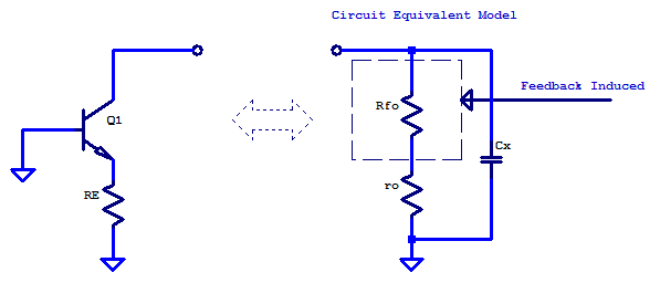
By inspection, the low frequency output resistance is
\[ R_{out} = r_o + R_{fo} \]
Solving for \( R_{fo} \) with the use of equation (GB.11) yields
\[ R_{fo} = \frac{r_\pi R_E}{r_\pi + R_E} + \left[ 1 + \frac{g_m R_E r_\pi }{r_\pi + R_E} \right] r_o – r_o \]
\[ R_{fo} \simeq \left[ \frac{ R_E }{r_\pi + R_E} \right] \beta r_o \]
The circuit equivalent model’s pole will occur at
\[ p_a = \frac{-1}{\left( r_o+ R_{fo} \right) C_x} \]
Equating \( p_a \) to dominant pole \( p_1 \) and solving for \(C_x\)
\[ \frac{-1}{\left( r_o+R_{fo}\right) C_x} = \dfrac{ -1 }{ C_u \left[ 1 + \beta\left( \frac{R_E}{r_\pi + R_E} \right) \right] r_o }\]
\[ C_x = C_\mu \]
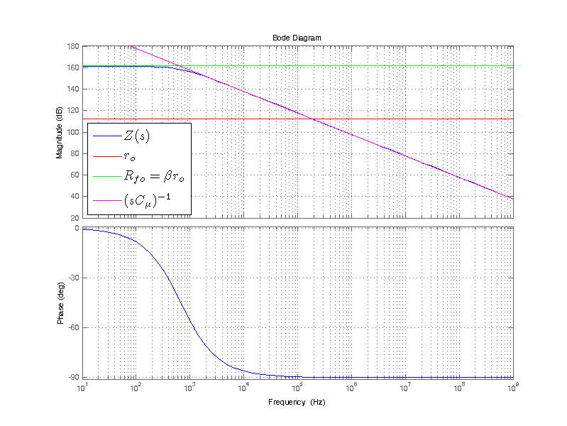
A comparison of \(Z(s)\) to the impedance of the circuit equivalent model can be seen on the bode plot below. The output impedance \(Z(s)\) of a CE amplifier with a low impedance source is plotted in blue. Impedance of each of the intrinsic elements and feedback equivalent element \(R_{fo}\) are plotted as well. As the emitter resistance \(R_E\) is increased the low-frequency output impedance pushes up from \(r_o\) towards a maximum of \(\beta r_o\).
While not covered analytically in this post, if a bypass capacitor were added in parallel to \(R_E\) (assuming the bypass capacitor is large), a break in low-frequency output impedance would occur. When the impedance of \(|Z_{C,bypass}|\) equals \(R_E\) the low frequency output impedance will begin to collapse at -20 dB/dec. This continues until the output impedance reaches the transistor’s intrinsic output resistance \(r_o\). After which, the output impedance appears as if \(R_E = 0\).
Spice Simulation Study
One challenge in a parametric study on the impact of Re and Rs to the output impedance of a CE amplifier is a potential shift in the DC bias point. If one were to use voltage or current sources which were not dependent on the choice of Re and Rs, the DC bias point will most like vary with changes in Re or Rs. A sample spice test jig to overcome this problem is the following:
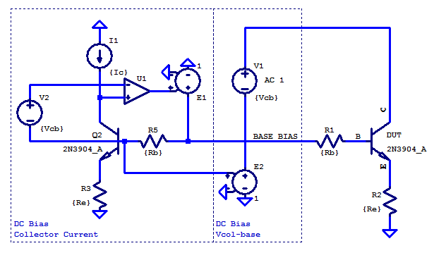
Here a current source I1 and voltage source V2 provide the desired operating point as collector current Ic and base-collector potential Vbc respectively. Amplifier U1 servos the base voltage to yield the desired operating point of Ic and Vcb. U1 is a idealized operational amplifier with 120dB open-loop gain and a Gain-BandWidth (GBW) of 1 Hz. A GBW product of 1 Hz is chosen as an extremely dominant pole compensation strategy. The output impedance of the test jig presented to the circuit under test is an ideal AC-ground (0 Ohms). The small-signal parameters gm,ro,Cu,Cpi are all a function of the DC operating point of Ic and Vbc. When gm,ro,Cu,Cpi are all held constant the output impedance as a function of Re, Rs, or both can be readily observed in a spice simulation. Stability of collector current bias for this test jig can be seen in the table below for Ic=250uA and various combinations of Re and Rs:
|
Re [Ohms] |
|||||||||||
| 1 | 10 | 100 | 1k | 10k | 100k | 400k | 1M | 10M | 100M | ||
|
Rb [Ohms |
1 |
10 pA |
0 |
0 |
10 pA |
0 |
0 |
0 |
0 |
0 |
0 |
| 10 |
10 pA |
-10 pA |
0 |
-10 pA |
0 |
0 |
0 |
0 |
0 |
0 |
|
| 100 |
0 |
0 |
0 |
0 |
0 |
0 |
0 |
0 |
0 |
0 |
|
| 1k |
0 |
0 |
0 |
0 |
0 |
0 |
0 |
0 |
0 |
0 |
|
| 10k |
0 |
0 |
0 |
0 |
0 |
0 |
0 |
0 |
0 |
0 |
|
| 100k |
0 |
0 |
0 |
0 |
0 |
0 |
0 |
0 |
0 |
0 |
|
A variation of \(\pm 0.25\) ppm in collector current was observed for Ic = 250 uA. Note that for Ic = 250 uA and Re = 100 MOhms, resistor Re is biased with 25 kVDC. Of course this is an idealized scenario, as such large values of Re would not be derived with an actual resistor, but with an active load such as a current source with high output impedance. Fortunately in a spice simulation 25 kV across a resistor is not a problem (well, maybe a tad for single precision arithmetic). Biasing of base-collector junction was also maintained at 5 VDC to within a fraction of a ppm, agnostic of choice for Re or Rs.
The DC bias conditions for the DUT can be any sensible value of temperature and collector current. For ease of mental arithmetic a simulation temperature of \(16.96 \;\mathrm{[^oC]}\) is chosen to set VT as 25 mV or (1/40 V).
\[ Tsim = \left(0.025 \frac{q}{k} – 273.15 \right) = 16.96 \;\mathrm{[^oC]} \]
Collector current is chosen such that \(g_m = 1/100 \) [A/V]
\[ I_C = VT g_m = 250 \;\mathrm{[\mu A]} \; = 1/4000 \;\mathrm{[A]} \]
The remaining small signal parameters also become easy to manipulate with mental arithmetic.
\[ r_\pi= \frac{1}{g_m} \beta = 100 \cdot 300 = 30 \;\mathrm{ k \Omega } \]
\[ r_o = \frac{ |VA|}{I_C} = 100 \cdot 4000 = 400 \;\mathrm{ k \Omega } \]
Note that the intrinsic output resistance is sometimes modelled as
\[ r_o = \frac{ |VA| + V_{cb}}{I_C} = 105 \cdot 4000 = 420 \;\mathrm{ k \Omega }\]
Complete DC operating point for the device under test (DUT) Q_DUT:
| Name: | Qdut |
|---|---|
| Model: | 2n3904_a |
| Ib: | 8.36e-07 |
| Ic: | 2.50e-04 |
| Vbe: | 6.37e-01 |
| Vbc: | -5.00e+00 |
| Vce: | 5.64e+00 |
| BetaDC: | 2.99e+02 |
| Gm: | 9.99e-03 |
| Rpi: | 2.99e+04 |
| Rx: | 0.00e+00 |
| Ro: | 4.20e+05 |
| Cbe: | 1.62e-11 |
| Cbc: | 2.04e-12 |
| Cjs: | 0.00e+00 |
| BetaAC: | 2.99e+02 |
| Cbx: | 0.00e+00 |
| Ft: | 8.73e+07 |
AC voltage source V1 drives the collector of the circuit under test, which results in an AC current directly related to output impedance. Output impedance of the circuit under test is then the following
\[Z_{out} = V(C)/I_C(DUT) \]
A sample plot of output impedance is the following:
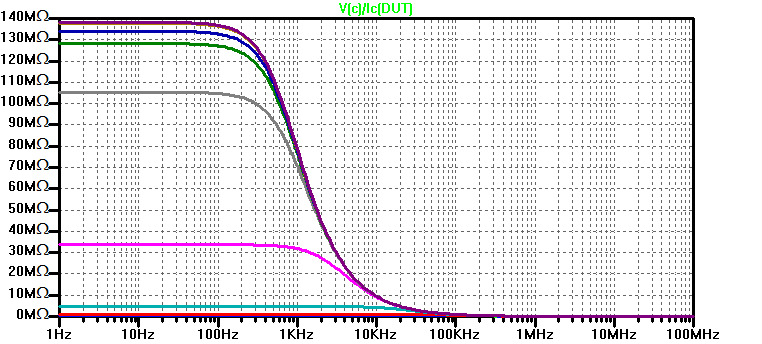
The red trace is for the lowest value of Re = 10 Ohms and the grey trace depicts the largest value of Re = 100 MOhms. In agrement with the previous analysis, the output impedance reaches a maximum value of \( \beta r_o \) for very large values of Re. Plotting output resistance on a linear scale was done to emphasize the significance of Re on output resistance. In the following figure the output resistance is plotted on a log-scale for a single spot frequency of 1 Hz.
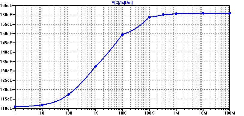
The intrinsic output resistance \(r_o\) of the DUT at 1 Hz is Va/Ic = 112 dBOhms, which coincides with the output resistance for Re ~ 0. For extremely large values of Re, an approximate 50 dB increase of output resistance near DC (\(f_{test}\) = 1 Hz) can observed from the plot. As discussed in the non-reactive model, the maximum increase in output resistance is a factor of \(\beta\).
\[ +50 \text{ dB} =10^{(50/20)} \simeq \beta \]
Referencing the spice DC operating point table above, for this simulation, \(beta = 299 \). A full comparison of the low-frequency model (\ref{LF.1}) to a spice simulation is shown in the figure below.
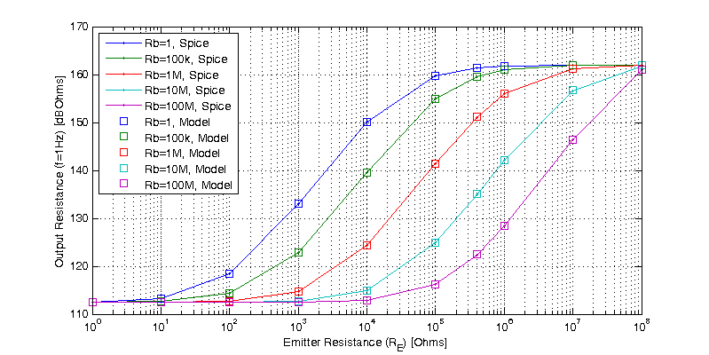
Recalling that \(1/gm = 100\) Ohms, looking at the figure above, for each multiple of \(1/g_m\) a 1x improvement in output resistance is realized. For \(Re=100\) Ohms the output resistance is doubled. For \(Re=10 \cdot 100\) Ohms the output resistance is increased 10x or 20 dB.
Interestingly, if a second transistor is stacked in series with the output of a CE amplifier (resulting in a cascode configuration), the second transistor will be biased with approximately the same collector current. 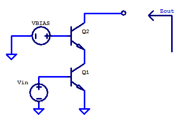
Likewise, having roughly all the same small-signal parameters. For the second transistor its base is tied to an ac-ground, and its emitter sees the output resistance of the CE amplifier. The intrinsic output resistance \(r_o\) is roughly 4000 times greater than \(1/gm\), for any value of collector current. The significance of using \(r_o\) for emitter degeneration can be seen in the figure above looking at the data point for \(Re=r_o=400\) kOhms, here the output resistance is only 5% percent away from the highest possible output resistance (when \(Re=\infty\)). Formally the second transistor is operating as a common-base amplifier, however the analysis presented here fully applies.
AC-Grounded Emitter
A spice simulation with a parametric sweep of source resistance is shown in the figure below. Source resistance was swept logarithmically from 1 Ohm to 100 MOhm in 1 decade steps.
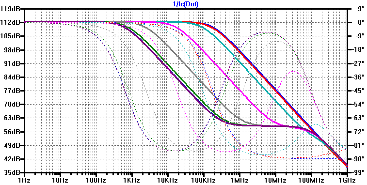
Graphically analyzing the output impedance, two poles and one zero exist, with the second pole always occurring at around 100 MHz. The first pole and single zero translate lower in frequency as the source resistance is increased. A comparison of the poles and zeros estimated from Z(s) (GE.10) to those estimated in the spice simulation can be observed in the figure below.
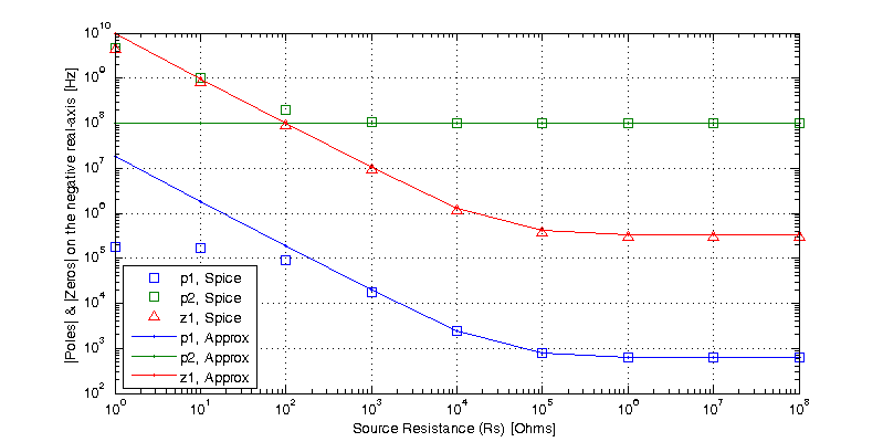
Recalling that the approximate poles and zeros are
\[z_1 \simeq \dfrac{-\left( r_\pi + R_S \right)}{ r_\pi R_S C_\pi }, \;\;\; p_1 \simeq \dfrac{-\left(r_\pi + R_S \right)}{g_m R_S r_\pi r_o C_\mu}, \;\;\; p_2 \simeq \dfrac{-g_m}{C_\pi} \]
A comparison of the circuit equivalent model created for the grounded-emitter case versus the spice simulation is shown in the figure below.
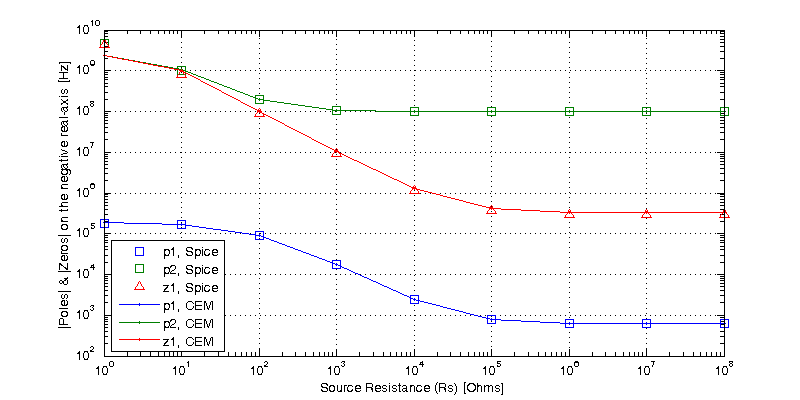
When the pole-zero pair are closely located, they approximately cancel, making it difficult to numerically solve an accurate absolute value. When the pole and zero begin to separate, the numerical estimate from the spice simulation shows good agreement with the poles and zero of the circuit equivalent model.
AC-Grounded Base
Using the same spice test jig as above, a parametric sweep of emitter resistance is performed. Emitter resistance is swept logarithmically from 1 ohm to 100 MOhm in 1 decade steps. From the simulation results, output impedance as a function of emitter resistance is shown in the figure below.
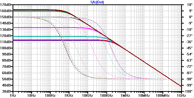
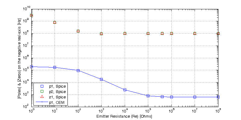
Noting that the output impedance breaks at a single frequency and continues to decline at -20dB/dec indefinitely, meaning Z(s) is approximately a single pole function. Recall from the grounded-base section, that the approximate poles and zero were found to be
\[p_1 \simeq \dfrac{ -1 }{ C_u \left[ 1 + \beta\left( \frac{R_E}{r_\pi + R_E} \right) \right] r_o }, \;\;\;\; p_2 = z_1 \simeq – \dfrac{r_o + R_E + g_m R_E r_o}{ R_E r_o C_\pi} \]
A comparison of the hand approximated poles and zero of \(Z(s)\) to those seen in the spice simulation is shown in the figure below.
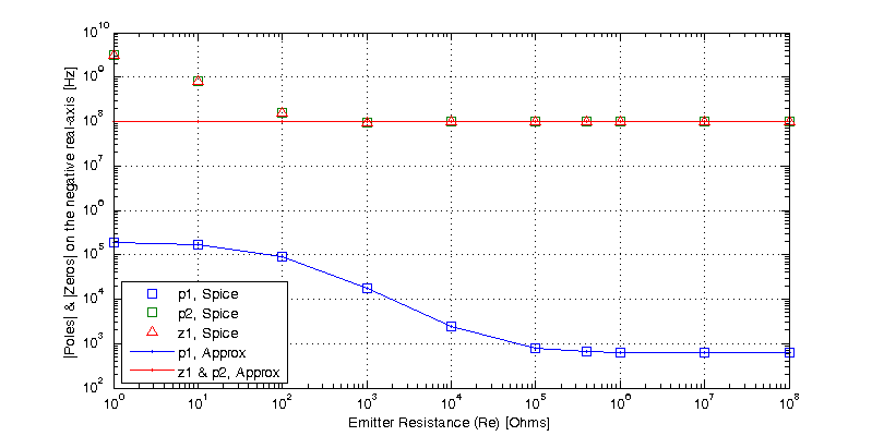
The circuit equivalent model for the grounded-base has only a single pole and no zeros. A comparison of the CEM’s dominant pole to the poles and zeros observed in the spice simulation is shown in the figure below.
