In this post we will develop and analyze a practical “type 2” error amplifier. The distinction of “type” 1, 2, or 3, is merely a description of how many poles are present in the compensator. All three types of error amplifiers will attempt to employ a pole at DC, i.e. operate as an integrator at low frequencies. Of course an error amplifier with an ideal integrator has a steady-state error of zero. However as is almost to all to common, digi-key does not stock any textbook class op-amps, with infinite differential gain and endless amounts of bandwidth.
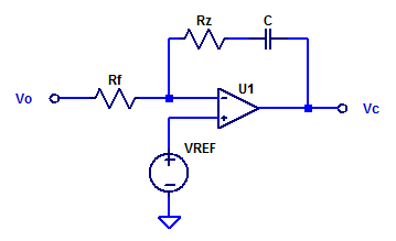
The figure below illustrates a practical type 2 error amplifier with voltage input and voltage output.

The output is sensed via feedback resistor \(R_f\) and the set-point is provided by voltage source \(V_{REF}\) to the positive input terminal of amplifier U1.
Transfer Function
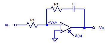
The voltage reference sets the DC operating point but its value has no impact on loop dynamics (provided its within the common-mode of the error amplifier). As a result, the schematic can be simplified as shown in the figure below to develop the transfer function.

We first note that the the amplifier is non-ideal, having its own open-loop transfer function \(A(s)\). Provided one employs an op-amp which is advertised as being unity-gain stable (most are), a simplified model for \(A(s)\) is the following,
\[ A(s) = \dfrac{A_{ol}}{1-\dfrac{s}{p_a}} \]
where the single dominant pole occurs at
\begin{align*}
p_a &= -\dfrac{\text{GBWP}}{A_{ol}} \;\; [\text{Hz}] \\
p_a &= -\dfrac{\text{GBWP}}{A_{ol}} 2\pi \;\; [\text{rad/s}]
\end{align*}
We can relate the input terminal potential of the opamp to its output as
\[ V_o = – V_x A(s) \]
Note the negative as the input is on the inverting terminal.
Applying KCL at the intermediate node \(V_x\) as,
\[ \dfrac{V_x-V_i}{R_f} + \dfrac{V_x-V_o}{R_z + 1/sC} = 0 \]
\[ V_x\left( \dfrac{1}{R_f} + \dfrac{1}{R_z+1/sC} \right) – \dfrac{V_i}{R_f} – \dfrac{V_o}{R_z + 1/sC} = 0 \]
Substituting the op-amps open-loop gain yeilds,
\begin{align*}
V_x &= \dfrac{-V_o}{A(s)}\\
V_x &= \dfrac{-V_o\left( 1 – s/p_a\right)}{A_{ol}}
\end{align*}
Substitution of \( V_x \),
\[ \dfrac{-V_o\left( 1 – s/p_a\right)}{A_{ol}} \left( \dfrac{R_f+R_z+1/sC}{R_f(R_z+1/sC)} \right) – \dfrac{V_o}{R_z + 1/sC} = \dfrac{V_i}{R_f} \]
\[ \dfrac{-V_o}{R_f(R_z+1/sC)} \left( \dfrac{\left( 1 – s/p_a\right)\left(R_f+R_z+1/sC\right)}{A_{ol}} -R_f\right) = \dfrac{V_i}{R_f} \]
\[ V_o\left( \dfrac{\left( 1 – s/p_a\right)\left(R_f+R_z+1/sC\right) + A_{ol}R_f}{A_{ol}} \right) = -V_i(R_z+1/sC) \]
Finally the transfer function becomes,
\begin{align*}
\dfrac{V_o}{V_i} &= \dfrac{-A_{ol}(R_z+1/sC)}{A_{ol}R_f + R_f + R_z – \dfrac{1}{Cp_a} + \dfrac{1}{sC} – \dfrac{s(R_f+R_z)}{p_a} } \\ \\
H(s) &= \dfrac{-A_{ol}(1 + sR_zC)}{1 + s\left( -1/p_a +C\left( R_f + R_z + A_{ol}R_f \right)\right) – \dfrac{s^2C(R_f+R_z)}{p_a} } \\
\end{align*}
The one zero occurs at
\[ z_1 = \dfrac{-1}{R_zC} \]
If we assume the poles are well separated, the dominate pole can be approximated as,
\[ p_1 \simeq \dfrac{-1}{-1/p_a +C\left( R_f + R_z + A_{ol}R_f \right)} \]
The dominate pole can be further simplified as,
\[ p_1 \simeq \dfrac{-1}{A_{ol}R_fC} \]
However \(|p_1|\) can never be greater than the intrinsic op-amp pole \(|p_a|\).
The second pole then occurs at,
\[ p_2 = \dfrac{p_aA_{ol}R_fC}{C(R_z+R_f)} \]
\[ p_2 = A_{ol}\left( \dfrac{R_f}{R_z+R_f} \right) p_a\]
The approximate transfer function is then,
\[ H(s) = \dfrac{-A_{ol}(1 – s/z_1)}{(1 – s/p_1)(1 – s/p_2)} \]
Amplifier Limitations
For the purposes of discussion, consider an error amplifier with the following parameters,
\begin{align*}
R_f &= 2 \text{ k}\Omega \\
R_z &= 100 \text{ k}\Omega \\
C &= 628 \text{ pF} \\
A_{ol} &= 100 \text{ dB} \\
\text{GBWP} &= 10 \text{ MHz} \\
\end{align*}
The exact transfer function is,
\[ H(s) = \dfrac{-(100000+ 6.28 s )}{1+0.1273 s+1.019\text{e-}007 s^2 } \]
With poles and a zero of
\[ z_1 = -2.534 \text{ [kHz]},\;\;\; p_1 = -1.251 \text{ [Hz]},\;\;\; p_2 = -198.7\text{ [kHz]}\]
The approximated poles and zero as developed above is the following
\[ \hat{z_1} = -2.534 \text{ [kHz]},\;\;\; \hat{p_1} = -1.267 \text{ [Hz]},\;\;\; \hat{p_2} = -196.1\text{ [kHz]}\]
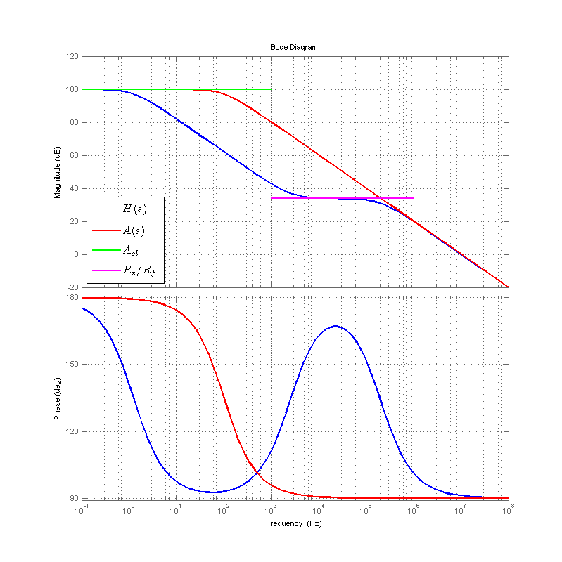
A bode plot of the transfer function of this sample type 2 error amplifier is shown in the figure below. Additionally the open-loop gain of the employed op-amp \(A(s)\) is also included.

We can see that, the blue trace \(H(s)\), resembles the classic type 2 error amplifier as having a pole near DC, and a mid-band region of phase boost. However it should also be apparent that the error amplifier cannot provide a response greater than that of the open-loop gain of the op-amp \(A(s)\). As a result, we can not actually place a pole at DC, as we would require an op-amp with infinite open-loop gain \(A_{ol}\).
We are free to choose an arbitrary location of the zero of the error amplifier. Following a choice for \(z_1\) we may choose only one of the following secondarily,
– Pole location \(p_1\)
– Pole location \(p_2\)
– Error amplifier gain during phase boost
The two hallmark specifications of an op-amp regarding loop dynamics are open-loop gain \(A_{ol}\) and Gain-BandWidth product. A typical open-loop gain for an op-amp is 100 dB, however some are available with 120 dB or even 150 dB of open-loop gain. The GBWP is also the unity gain crossover frequency of the amplifier, which declines at a rate of 20 dB/dec for the single pole model.
This post focused on loop dynamics, however as will be seen in a future post, a plethora of other op-amp specifications are also important for its steady state and dynamic performance, such as input offset voltage, common-mode rejection, power-supply rejection, temperature coefficients, input-bias currents, input-referred noise, and others…
Kiváló webhely van itt… Manapság nehéz olyan jó minőségű írást találni, mint az Öné.
Nagyon nagyra értékelem az olyan egyéneket, mint te!
Vigyázz magadra!!