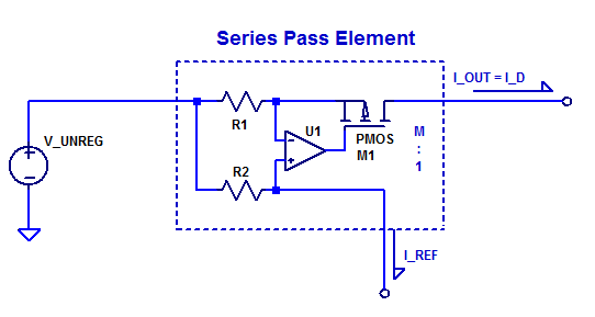
The role of the series pass element is to supply a regulated current \( I_{out}\) from the unregulated input supply to the output load of the LDO. A simplified model of a current-mode series pass element is shown below.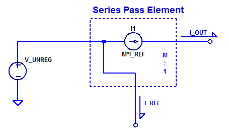
A single input \( I_{REF}\) modulates the current source which supplies an output current \( I_{OUT}\). One may observe the similarity of this element to that of a current mirror where transistor geometry scaling provides a 1 to \(M\) current mirror ratio. In fact, a current mirror is one plausible circuit implementation for a current-mode series pass element. However, an even simpler circuit implementation is a single PNP bipolar transistor. A schematic of a PNP BJT pass element is shown in the schematic below.
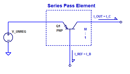
At low-frequencies the output load current delivered by the collector of Q1 is simply,
$$ I_C = \beta I_B $$
Equivalently,
$$ I_{out} = \beta I_{ref} $$
Transfer Function
A small-signal schematic of the PNP BJT current-mode series pass element is shown in the figure below.
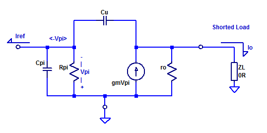
Since \(Z_L = 0\), i.e. the output is grounded, the small-signal schematic can be simplified as,
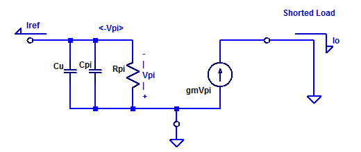
$$ V_{\pi} = I_{ref} \left( r_\pi || \left(\dfrac{1}{s(C_\pi + C_\mu )}\right)\right) $$
For simplicity combine both capacitors as,
$$ C = C_\pi + C_\mu $$
$$ V_\pi = I_{ref} \dfrac{r_\pi}{1 + s r_\pi C} $$
At the collector of the PNP pass-element we have,
$$ V_o = I_o Z_L $$
Since \( Z_L \approx 0 \), the output voltage is
$$ V_o = 0 $$
Hence, the pass element is being driven into an AC-ground. For a typical linear regulator with significant output bulk and bypass capacitors (potentially in the 10’s of microFarads), this a good approximation.
\begin{align*}
I_o &= g_m V_\pi \\
&= (g_m)(I_{ref}) \dfrac{r_\pi}{1 + s r_\pi C} \\
&= \dfrac{g_m r_\pi}{1 + s r_\pi C} I_{ref}
\end{align*}
Substituting small signal model parameter \(r_\pi = \beta/g_m\) yields,
\begin{align*}
I_o &= \dfrac{g_m (\beta/g_m)}{1 + s (\beta/g_m) (g_m \tau_f + C_\mu) } I_{ref}\\
I_o &= \dfrac{\beta}{1 + s \beta(\tau_f + C_\mu/g_m) } I_{ref}
\end{align*}
The transfer function of \( I_o ( I_{ref}) \) has no zeros and one pole at,
$$ p_a = \dfrac{-1}{\beta( \tau_f + C_\mu/g_m )} $$
When \( g_m \) is large the pole occurs at
$$ p_a \simeq \dfrac{-1}{\beta \tau_f } $$
As an example consider a 2N3906 operating as a series pass element. Assume the PNP transistor has a \(\beta = 200\) and a \( \tau_f = 350 \) ps. The current gain transfer function would then have a pole at,
$$ p_a = \dfrac{-1}{200 \cdot 350 E-12} = – 14.3 \textrm{Mrad/s} = -2.3 \textrm{MHz}$$
A complete plot of the current gain bandwidth of a 2N3906 into a short-circuit load is shown in the figure below.
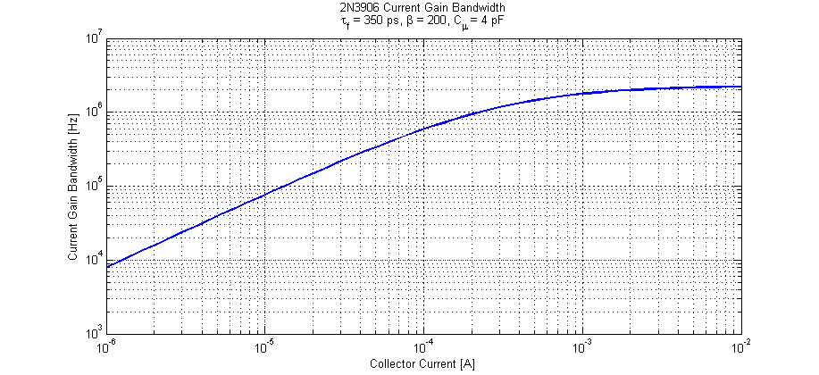
We can note that for collector currents greater than \(\approx 1 \) mA the transistor achieves its maximal current gain bandwidth. From a controls perspective, if we maintain a minimum load current of 1 mA the transistor will have negligible phase perturbations within the control bandwidth (sub 1 MHz).
Spice Simulation
Consider the following simplified test jig of a PNP series pass element shown in the figure below. An AC test current source is applied to the base and the collector terminal is biased such that the transistor is in active mode. A simplified model of a 2N3906 is employed which only includes the diffusion capacitance of the base-emitter junction ( \( g_m \tau_f \) ), depletion capacitance was omitted to match analysis above.
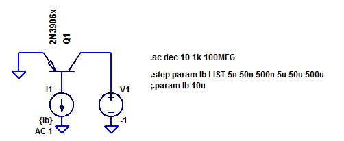
Collector current is parametericly stepped from \( \approx 1\) uA to \( \approx 100 \) mA in 1 decade steps. The AC current gain of Q1 is plotted in the bode plot below.
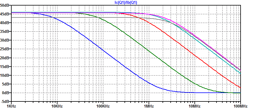
Note the transition frequency \(f_t\) (unity current gain into shorted-load) is well above 100 MHz for collector currents above 100 \(\mu\text{A}\).
The current gain is plotted again focusing on the 3 dB break points for various collector current biasing points. A maximum current-gain bandwidth of 3 MHz is realized for collector currents greater than 1 mA.
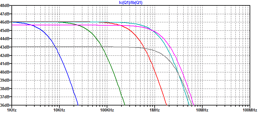
The subtle difference in bandwidth between the analytical expression derived above and the spice simulation is due to C-V modulation of the base-collector junction. As the base-collector junction is further reverse biased, the depletion width expands and as a result the net depletion capacitance reduces. This behavior can be advantageously exploited by the designer or marketer (in specsmanship). A transistor will have a considerably higher low-current \(f_t\) when the collector is biased at a large DC potential (reduction of \(C_\mu\) and larger \(\beta\) from base-width modulation).
Alternate Series Pass Element Implementations
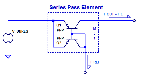
Current Mirror
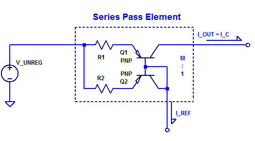
Emitter Degenerated Current Mirror
Q1 and Q2 do not need to be geometrically matched or isothermal to each other. Resistors R1 and R2 set the current mirror ratio as R1/R2 (neglecting base current).
MOSFET Active Current Mirror
