In this post, the exact transfer function of an R2R DAC will be developed for arbitrary ladder resistors and voltage references. An R2R DAC which has separate positive and negative references is shown in the figure below.
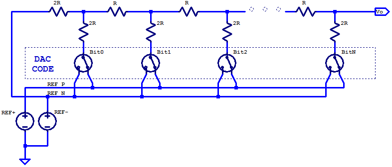
We can observe that if \( V_{REFN} = \text{GND} \), the schematic is equivalent to the previous definition of a general R2R DAC. In practice, the range of permissible voltages for \(V_{REFN}\) and \(V_{REFP}\) depend on the voltage ratings of the switching elements utilized. If DAC sample rate was of no concern, mechanical relays could be employed as the switching elements (which can tolerate a wide range of common mode voltages from the contacts to switching coil). The combination of switching elements and voltage references can be simplified as programmable voltages sources as shown in the schematic below.
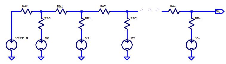
From the previous post, the unloaded voltage of the first ladder element can be solved as a simple voltage divider between two nodes, which yields,
\[ V_0′ = \dfrac{R_{B0}V_{REFN} +R_{A0}V_0 }{R_{A0} + R_{B0}} \]
The output resistance of ladder node at bit0 is
\[ R_0 = R_{A0} || R_{B0} \]
Continuing onto the second bit, bit1 in the ladder, we replace bit0 ladder elements as a Thevenin equivalent circuit, as shown in the figure below.
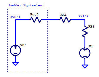
Applying KCL at the \( V_1’\) node yields,
\[ \dfrac{V_1′ – V_0′}{R_{o,0} + R_{A1}} + \dfrac{V_1′ – V_1}{R_{B1}} = 0\]
With some basic algebra, the unloaded ladder potential can be solved as,
\begin{align*}
V_1′ \left( \dfrac{1}{R_{o,0} + R_{A1}} + \dfrac{1}{R_{B1}} \right) &= \dfrac{V_1}{R_{B1}} + \dfrac{V_0′}{R_{o,0} + R_{A1}} \\
V_1′ \left( \dfrac{R_{o,0} + R_{A1} + R_{B1}}{(R_{B1})(R_{o,0} + R_{A1})} \right) &= \dfrac{V_1}{R_{B1}} + \dfrac{V_0′}{R_{o,0} + R_{A1}} \\ \\
V_1′ &= \dfrac{R_{B1}V_0′ + (R_{o,0} + R_{A1})V_1 }{R_{o,0} + R_{A1} + R_{B1}}\\
\end{align*}
The output resistance looking into node at bit1 in the ladder is by inspection,
\[ R_1 = \dfrac{(R_{o,0}+R_{A1})R_{B1}}{ R_{o,0} + R_{A1} + R_{B1}} \]
The solution for the nth element in the ladder is then found by simplifying the n-1 ladder elements as shown in the figure below,
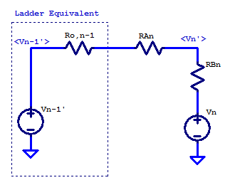
Applying KCL at the \( V_n’\) node yields,
\[ \dfrac{V_n’ – V_{n-1}’}{R_{o,n-1} + R_{An}} + \dfrac{V_n’ – V_n}{R_{Bn}} = 0\]
\begin{align*}
V_n’ \left( \dfrac{1}{R_{o,n-1} + R_{An}} + \dfrac{1}{R_{Bn}} \right) &= \dfrac{V_n}{R_{Bn}} + \dfrac{V_{n-1}’}{R_{o,n-1} + R_{An}} \\
V_n’ \left( \dfrac{R_{o,n-1} + R_{An} + R_{Bn}}{(R_{Bn})(R_{o,n-1} + R_{An})} \right) &= \dfrac{V_1}{R_{Bn}} + \dfrac{V_{n-1}’}{R_{o,n-1} + R_{An}} \\ \\
V_n’ &= \dfrac{R_{Bn}V_{n-1}’ + (R_{o,n-1} + R_{An})V_n }{R_{o,n-1} + R_{An} + R_{Bn}} \\
\end{align*}
We can see that by iterating down the ladder the complete solution can be found for an n-bit R2R DAC.
Sample Matlab code for calculating an R2R DAC’s output voltage given arbitrary ladder resistors and voltage references is shown in the listing below.
N = 8; % 8-bit R2R DAC

RA = 1000*ones(N,1);
RB = 2000*ones(N,1);
RA(1) = 2000;

VrefP = 5; % Positive Reference Voltage [V]

VrefN = 0; % Positive Reference Voltage [V]

DACcode = 128; % Mid-scale DAC code

% Binary code of DAC
binCode = dec2bin(DACcode,N);

% Reference Switch states
SWn = binCode(end:-1:1) == '1';

% Pre-allocate variables for ladder nodes
Vn = nan(N,1);
Rn = nan(N,1);

% Iterate through R2R ladder starting a bit0
%   Matlab indexing starts at 1
for i = 1:N
  if i == 1
    % First bit in ladder, no lower elements
    % Output resistance
    Rn(i) = RA(i)*RB(i)/(RA(i) + RB(i));

    % Unloaded ladder voltage
    Vn(i) = ( (VrefP*SWn(1) + VrefN*~SWn(1))*(RA(1)) ...
                + RB(1)*VrefN )/(RA(1)+RB(1));
  else
    % 2nd to nth ladder bits
    % Output resistance
    Rn(i) = (Rn(i-1) + RA(i))*RB(i)/(Rn(i-1) + RA(i) + RB(i));

    % Unloaded ladder voltage
    Vn(i) = ((VrefP*SWn(i) + VrefN*~SWn(i))*(RA(i) + Rn(i-1)) ...
    + RB(i)*Vn(i-1) )/(Rn(i-1) + RA(i) + RB(i));
  end
end

Vdac = Vn(end);
Spice Simulation
Here we will compare a the analytic solution developed above to that of a spice simulation using a prototype DAC constructed with low-tolerance resistors. Ladder resistors \(R_{Ai}\) and \(R_{Bi}\) have a nominal resistance of 1 \(k\Omega\) and 2 \( k\Omega\) respectively. Both resistor sets \(R_{Ai}\) and \(R_{Bi}\) are mismatched randomly. Each resistor has an error \( \delta R\) drawn from normal distribution with a standard deviation of 5% of the resistors nominal value.
\begin{align*}
R_{Ai} &\sim \mathcal{N}\left( 1000, (50)^2 \right) \\
R_{Bi} &\sim \mathcal{N}\left( 2000, (100)^2 \right) \\
\end{align*}
One sample set of resistors is shown in the table below.
| Bit | RAx [Ohms] | RBx [Ohms] |
|---|---|---|
| 0 | 2076 | 1953 |
| 1 | 1034 | 1956 |
| 2 | 1080 | 2145 |
| 3 | 1061 | 1987 |
| 4 | 1023 | 1842 |
| 5 | 972 | 1781 |
| 6 | 986 | 2025 |
| 7 | 1026 | 1952 |
The LTSpice schematic of the proposed DAC is shown in the figure below.
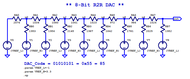
The two reference voltages chosen arbitrarily to be,
\begin{align*}
V_{REF,P} &= 3.3 \text{ V} \\
V_{REF,N} &= -1 \text{ V} \\
\end{align*}
A sample DAC code of \(0\texttt{x}55\) is chosen arbitrarily, which is \(0\texttt{b}01010101\) in binary and \(85\) in decimal. The DC operating point solution generated by LTSpice is shown in the table below. Note that, the intermediate ladder node voltages are the loaded potentials. With the exception of the final output node being unloaded, which matches the analysis presented above.
| Spice Node | DC Voltage [V] |
|---|---|
| V(n0) | 0.929927 |
| V(n1) | 0.636357 |
| V(n2) | 1.23324 |
| V(n3) | 0.797312 |
| V(n4) | 1.30234 |
| V(n5) | 0.728053 |
| V(n6) | 1.10218 |
| V(out) | 0.377923 |
Using the Matlab/Octave sample code above, one can find the solution to be
\[ V_{DAC} = 0.377923 \text{ V} \]
The iterative analytical solution developed above is identical to that produced in spice (a simultaneous matrix solution vs the iterative solution developed here).
The scale factor of the proposed DAC is the total output span divided by the number of DAC codes, i.e.
\[ \Delta LSB = \dfrac{ 3.3 – (-1)}{ 2^8} = 16.8 \text{ mV} \]
If the resistor elements were ideal, with exact values of 1 \( k\Omega\) and 2 \( k\Omega\), then the ideal output for the DAC at code \(85\) would be
\[ V_o = -1 + 85(\Delta LSB) = 427.7 \text{ mV} \]
Since the resistors used had finite tolerance, mismatches in the ladder cause the reposnse to deviate from the ideal case. The difference between ideal and actual is
\[ V_{error} = V_{DAC} – V_o = -49 \text{ mV} \]
This discrepancy of \(-49 \text{ mV}\) is solely due to the mismatch in the ladder resistors. It is customary to discuss DAC errors in terms of LSBs, as its provides a comparable figure of merit (for equal bit output DACs) without having to know what voltage references were used with the DAC. For this prototype DAC, at code \(85\) the output is in error by -2.9 LSB from the ideal response. Considering that some of the ladder resistors are in error by up to 10%, having a output that is only in error by 1.2% of full-scale-range, is a reasonable result.
To see the full picture, we can evaluate the DAC response over all output codes. For an 8-bit DAC the range of applicable output codes span from 0 to \(2^8-1 = 255\). The complete DC output response over all DAC codes is shown in the figure below.
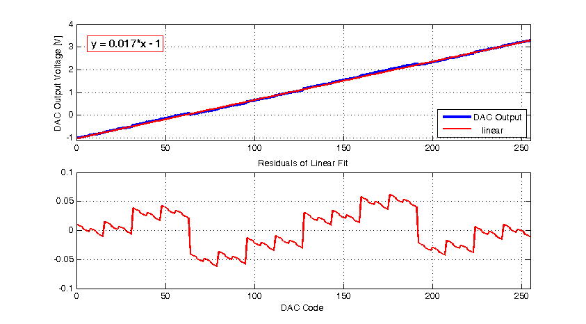
From the response above, we can see the DAC output is \( V_{REFN} = -1 \text{ V}\) at output code \( 0 \), as expected. When the DAC response is fit to a first order function, the slope is \( 17 \text{ mV/LSB}\), which is also approximately equal to the ideal response. Looking at the residuals from a first order fit, the response deviates from a linear response by up to \( \pm 60 \text{ mV} \). In LSB terms the maximum error is \(\pm 3.5\) LSB. In some ways, the results are positive, in that, for grossly mismatched resistors (upwards of 10%), the DAC’s response is maximally in error by 1.4% of full-scale-range. The DACs DC response near code 60 is shown in the figure below.
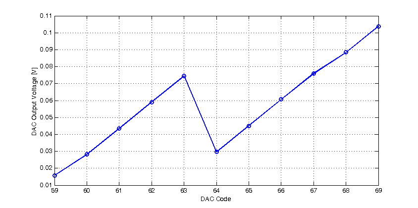
One of the alarming attributes of this DAC’s response, is that, upon transition from code 63 to 64, the output decreases! In fact, after code 63, it isn’t until code 67 that, the response is approximately equal to code 63. This behaviour is described as non-monoticity. Of all DAC characteristics, non-monoticity is one of the most severe, as it is difficult to compensate for. Hypothetically, if a DAC has an output offset voltage, one can add additional offset circuit to compensate for the fact. The same is also true for a DAC with scale error, an adjustable gain amplifier may be added to compensate for the DAC’s gain error. However correcting non-monoticity of a DAC is not a trivial solution, and thus, it is best practice to eliminate this behaviour in the first place.
In future posts, we will discuss how to avoid non-monoticity and other DAC characteristics.
Ciao ,it is nice. many thanks