In this post a sample schmitt-trigger relaxation oscillator is constructed and instrumented.
Measurement Setup
A simplified schematic of the test setup is shown in the figure below.
A tribute to the crustiest jellybean; and how powerful it still is.
In this post a sample schmitt-trigger relaxation oscillator is constructed and instrumented.
A simplified schematic of the test setup is shown in the figure below.
In a traditional oscillator, oscillation is achieved by providing a loop-gain greater than unity and a phase-shift of \(0^o\) at some \(f_{osc}\). However, in the case of a relaxation oscillator, oscillation is achieved by switching between two discrete states. Often a relaxation oscillator is constructed with a non-linear circuit element which can provide 2 threshold voltage levels to define two discrete states. One non-linear circuit element which is commonly employed in a relaxation oscillator is a schmitt trigger.
Due to the hysteresis developed internal to the schmitt trigger, two trigger thresholds are realized, namely \(V_N\) and \(V_P\). Where \(V_N\) is the negative threshold voltage and \(V_P\) is the positive threshold voltage. The hysteresis voltage is then,
$$ V_H = V_P – V_N $$
Ideally, the thresholds \(V_N\) and \(V_P\) would be centered around mid-supply (\(V_{dd}/2\)), however in practice this is only approximately true.
A minimal component count relaxation oscillator is shown in the figure below.
 Continue reading “CD40106 Schmitt Trigger Relaxation Oscillator”
Most of the datasheets from assorted suppliers of a 1N4148 diode all guarantee a maximum diode capacitance of 4 pF at \(V_D\) = 0 VDC. A sample excerpt from the Vishay datasheet has the \(C_D\) specification circled in red.
 Continue reading “1N4148 Diode Reverse Biased Junction Capacitance”
In this post the output drive characteristics of a Cd40106 are measured and analyzed. The drive strength of a gate is important in high-speed signaling in order to quickly charge/discharge PCB interconnect capacitance and the effective input capacitance of the receiving gates/ICs.
The datasheet’s specification for the CD40106’s output low current sink \(I_{OL}\) is shown in the figure below.

We can translate the typically sink current to an approximate resistance as,
$$ R_{OL,5} = \dfrac{V}{I} = {0.4}{0.001 } = 400 \; \Omega $$
From the datasheet we can calculated the typical output resistance for all 3 specified Vdd supply values as,
$$ R_{OL,5} = 400 \; \Omega \;\;\; R_{OL,10} = 192 \; \Omega \;\;\;R_{OL,15} = 221 \; \Omega $$
Note the output resistance is specified to be lower on a 10 V supply versus a 15 V supply. In the section below we will determine if indeed a 10 V supply yields the lowest output low resistance. Continue reading “CD40106 Output Drive Characteristics”
A schmitt-trigger to a first operates just like any digital buffer/inverter where a logic level input ( Gnd or Vdd ) yields some digital output value based on the logic function of the gate. What is different about an inverting schmitt-trigger over a basic inverter is the input threshold voltage changes depending on the gate’s output state. In the case of a schmitt-trigger the input threshold level receives a small positive feedback from the output. Hence when the output is triggered high, the input threshold voltage is boosted a small amount. Equivalently, when the output is low the input threshold voltage is lowered a small amount. This positive feedback of the output to the input is refereed to as hysteresis.
The transfers characteristics figure available from the CD40106 datasheet is shown below.

Continue reading “Schmitt-Trigger Threshold Levels (CD40106)”
In this blog post, the forward biased voltage-current relationship of a 1N4148 diode will be measured and analyzed.
Shockley in 1949, published a paper describing the behavior of a diode as,
$$ I_D = I_s \left( \exp \left( \dfrac{V_D}{\eta V_T}\right) -1 \right) $$
Where \( \eta \) is a constant representing the ideality of device, typical values of \( \eta \) range from 1 to 2 for silicon diodes.
$$ V_T = \dfrac{kT}{q} $$
At a room temperature of \(22\;^o\text{C}\) the thermal voltage is,
$$ V_T(22\;^o\text{C}) = \dfrac{(1.381\cdot 10^{-23})(273.15+22)}{1.602\cdot 10^{-19}} = 25.4 \text{ mV} $$ Continue reading “1N4148 Diode Forward Biased I-V Curve”
When a silicon diode is sufficiently reverse biased, the junction undergoes either avalanche or zener breakdown. Zener breakdown is a quantum mechanical behavior which typically occurs at potentials less than -5 V or -6 V for silicon diodes. Avalanche breakdown occurs when a thermally generated electron-hole pair is sufficiently accelerated by the reverse bias electrical field, such that, when they impact a second carrier they cause impact ionization. These additional free carriers then cause more impact ionization and this becomes a multiplicative process. Ultimately conducting high levels of current due to the multiplicative gains of avalanche breakdown.
Breakdown specifications taken from the 1N4148 datasheet are shown highlighted in the figure below.
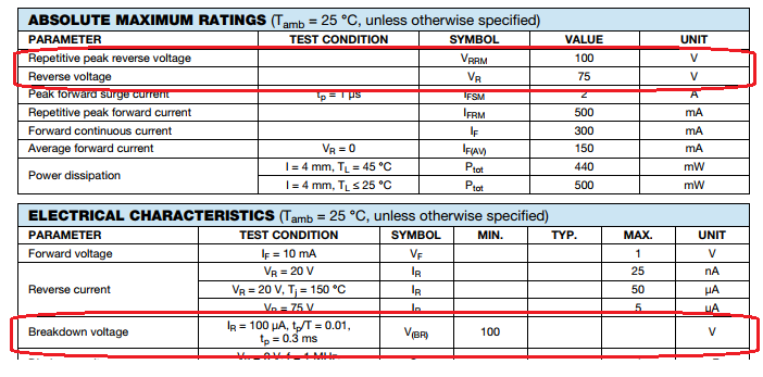
At room temperature, we expect to observe a breakdown voltage greater than 100 VDC. The recommended largest reverse working voltage is given as 75 VDC.
The standard spice model of a diode under reverse bias is the following,
\[
I_D =
\begin{cases}
I_s\left(e^{\eta qV_D/kT} -1 \right) + V_D\text{GMIN} &\quad\text{for} & -5\dfrac{\eta kT}{q} \leq V_D \leq 0 \\ \\
-I_s + V_D\text{GMIN} &\quad \text{for} & V_D < -5\dfrac{\eta kT}{q}\\ \\
-IBV & \quad \text{for} & V_D = -BV \\ \\
-I_S\left( e^{-q(BV+V_D)/kT}-1 + \dfrac{qBV}{kT}\right) & \quad \text{for} & V_D < – BV
\end{cases}
\]
All semi-conductor diodes have some amount of reverse-bias conductance. In the case of a 1N4148, reverse leakage current is guaranteed to be less than 25 nA when reverse-biased at -20 VDC at room temperature (25 degC). In this post we will measure the reverse biased I-V curve of 4 1N4148 diodes.
The standard spice model of a diode under reverse bias is the following,
\[
I_D =
\begin{cases}
I_s\left(e^{\eta qV_D/kT} -1 \right) + V_D\text{GMIN} &\quad\text{for} & -5\dfrac{\eta kT}{q} \leq V_D \leq 0 \\ \\
-I_s + V_D\text{GMIN} &\quad \text{for} & V_D < -5\dfrac{\eta kT}{q}\\
\end{cases}
\]
When the DUT is reverse biased from 0 mV to -250 mV, we expected to observe a large rise in leakage current. For reverse bias voltages less than -250 mV, we expect to see a constant current source with a high parallel resistance.
Continue reading “1N4148 Reverse Bias Leakage Current”
One most likely doesn’t need any assistance in recalling Ohm’s law as,
$$ V = I R $$
Or equivalently,
$$ I = \dfrac{V}{R} $$
Of course this is an idealized expression, as all resistors have a voltage coefficient due to self-heating. A resistor R will dissipate a power under load of
$$ P_d = I^2 R $$
The power dissipation leads to a temperature rise and the temperature coefficient of resistance material leads to a deviation in nominal resistance.
In this blog post, we will take a look at the I-V linearity of a handful of 1 kOhm resistors. Continue reading “Resistor I-V Linearity”
Continuing on from the analysis presented in low-noise-high-psrr-ldo-transconductance-gm-block, a simplistic trans-conductance amplifier can be constructed as shown in the figure below.

Forward trans-conductance from \( V_i \) to \( I_o \) was shown to be approximately,
$$ g_m = \dfrac{1}{R_E} \;\;\; \text{[A/V] } $$
For evaluation purposes, a \(g_m\) of 1 mA/V is chosen arbitrarily. The resistance of Re is then simply, Continue reading “Trans-conductance Amplifier Measurements”
