Low-Noise, High-PSRR LDO – Error Amplifier

In this post we will develop and analyze a practical “type 2” error amplifier. The distinction of “type” 1, 2, or 3, is merely a description of how many poles are present in the compensator. All three types of error amplifiers will attempt to employ a pole at DC, i.e. operate as an integrator at low frequencies. Of course an error amplifier with an ideal integrator has a steady-state error of zero. However as is almost to all to common, digi-key does not stock any textbook class op-amps, with infinite differential gain and endless amounts of bandwidth.

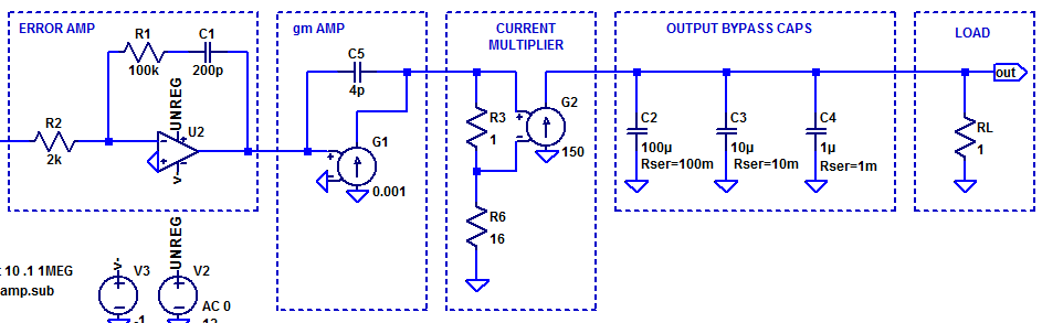
The figure below illustrates a practical type 2 error amplifier with voltage input and voltage output.

Practical Type 2 Error amplifier for use in a low-noise, high-PSRR LDO.

Continue reading “Low-Noise, High-PSRR LDO – Error Amplifier”

Low-Noise, High-PSRR LDO – Load Impedance

Unfortunately there are no “ideal” capacitors in the Digi-Key catalog (maybe one day). As a result, we must select a diverse set of capacitors to attempt to construct a closer to ideal capacitor. Each capacitor can be represented by an lumped element RLC model. While one can go to many ends to construct the best capacitor model, for the purposes of this blog post, we limit our capacitor to only including an equivalent series resistance (ESR). Since we are only concerned with frequencies below 1 to 10 MHz, a series inductance of a few nanohenries is discarded.

A sample output load for a Low DropOut regulator (LDO) is shown in the figure below.

Typical output load for an LDO

Continue reading “Low-Noise, High-PSRR LDO – Load Impedance”

DAC Specifications – Ideal Case

A Digital to Analog Converter (DAC) in the ideal case, provides a unique transform from a digital code to an analog voltage ratiometric to a supplied voltage reference. Several codings of the digital value are available. Two of the simplest codings are unsigned binary and unsigned fractional binary. Other possible codings include: two’s complement, sign-magnitude, one’s complement, and gray code. In practice, only unsigned binary and two’s complement (signed binary) are commonly employed in a DAC. For both the signed and unsigned cases, the integer and fractional codings share the same binary representation. For example, a 3-bit DAC has the response shown in the table below.

DAC Response to Integer and Fractional Codes
Decimal Fractional Unsigned Binary Fractional Binary DAC Output
0 0/8 000 0.000 \( 0/8 \; V_{REF} \)
1 1/8 001 0.001 \( 1/8 \; V_{REF} \)
2 2/8 010 0.010 \( 2/8 \; V_{REF} \)
3 3/8 011 0.011 \( 3/8 \; V_{REF} \)
4 4/8 100 0.100 \( 4/8 \; V_{REF} \)
5 5/8 101 0.101 \( 5/8 \; V_{REF} \)
6 6/8 110 0.110 \( 6/8 \; V_{REF} \)
7 7/8 111 0.111 \( 7/8 \; V_{REF} \)

Continue reading “DAC Specifications – Ideal Case”

R2R DAC

A Digital to Analog Converter (DAC) is a critical building block in almost every modern electronic system today. A DAC translates a digital code to an analog output voltage. For a typical uni-polar DAC, the DAC code maps to an output voltage spanning 0 V to the DAC’s associated voltage reference’s potential \(V_{REF}\). When a resistor ladder of two unique resistance quantities, namely R and 2R are chosen, some admirable attributes are obtained which are well suited to the design of a DAC. The schematic below is a simplified schematic of an R2R DAC; the DAC switches and voltage reference are idealized.

An N-bit R2R DAC, with single-ended unipolar output.

Continue reading “R2R DAC”

GPIO Output Resistance

In this blog post, we will take a look at the output resistance of General Purpose Input Output (GPIO) pins. For the purposes of discussion, the Microchip PIC24FJ32GA002; a 16-bit micro-controller available in a 28-pin DIP package, will be analyzed in detail related to its GPIO structure. In general for digital logical, three output states are available: output low, output high, and high-impedance. A simplified circuit for the output portion of a GPIO pin is shown below.Simplified schematic model of a GPIO pin.

Continue reading “GPIO Output Resistance”

LC Butterworth – Component Sensitivity

Monte-Carlo Simulation

Each of the discrete filter components is assumed to be normally distributed with \(\sigma = 0.02 \mu \).

\begin{align*}
R_S &\sim \mathcal{N}\left( 1, (0.02)^2 \right) \\
R_L &\sim \mathcal{N}\left( 1, (0.02)^2 \right) \\
L_1 &\sim \mathcal{N}\left( 1.6180, (1.6180 \cdot 0.02)^2 \right) \\
L_2 &\sim \mathcal{N}\left( 1.6180, (1.6180 \cdot 0.02)^2 \right) \\
C_1 &\sim \mathcal{N}\left( 0.6180, (0.6180 \cdot 0.02)^2 \right) \\
C_2 &\sim \mathcal{N}\left( 2, (2 \cdot 0.02)^2 \right) \\
C_3 &\sim \mathcal{N}\left( 0.6180, (0.6180 \cdot 0.02)^2 \right) \\
\end{align*}

Continue reading “LC Butterworth – Component Sensitivity”

LC Butterworth Filter

Physical synthesis of a Butterworth filter requires components which can be interconnected to form complex poles (dampened harmonic oscillators). A passive arrangement of resistors and capacitors can form arbitrary real valued poles and zeros; however a passive RC network cannot synthesize complex poles. The natural choice for passive components which can synthesize oscillators, are inductors and capacitors. An immediate benefit of choosing an LC network for synthesis, is that the network in the ideal case is lossless. Allowing for low insertion-loss in the pass-band, and maximizing power transfer from source to load.

The most common network structure for synthesis is a series inductor and shunt capacitor ladder. A LC ladder of arbitrary order \(n\), is shown in the figure below.

Schematic of an LC butterworth filter.

Continue reading “LC Butterworth Filter”